

Long-range nontopological edge currents in graphene
In search for novel and exotic transport phenomena (e.g. dissipationless spin and valley transport, topological currents, hydrodynamic flows etc.) nonlocal measurements are widely employed in the research on van der Waals heterostructures. In such experiments voltage is measured at contacts placed far away from the expected classical flow of charge carriers.
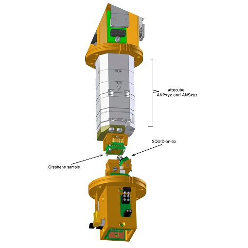
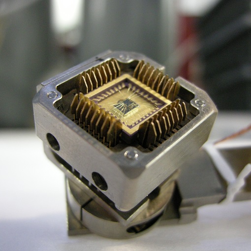
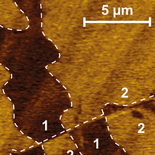
The group of Eli Zeldov (Weizmann Institute of Science, Israel), in collaboration with the group of Andre Geim (University of Manchester, UK) and Leonid Levitov (MIT, USA), has examined a giant nonlocality observed in charge-neutral graphene in the presence of magnetic field. Thermal imaging and scanning gate microscopy were done utilizing SQUID-on-tip with the help of the biaxial attocube scanner ANSxy100. It was the perfect fit due to its size, non-magnetic body, and scan range, that enables scanning of large devices under strong magnetic fields.
The Zeldov group imaged exotic flow patterns of long-range nonlocal currents, resulting from the commonly occurring charge accumulation at graphene edges. This mechanism is generic and nontopological, and is expected to support nonlocal transport in many electronic systems.
This measurement was realized with the ANSxy100lr/LT/HV xy-Scanner made from Titanium.
Further reading:
A. Aharon-Steinberg et al., Nature 593, 528 (2021)
G-Factor Anistropy Examined in High Magnetic Fields & at 200 mK
In a collaboration of the Zumbuhl Group with RIKEN, SAS and UCSB an experiment for showing the separation of the isotropic and anisotropic g-factor corrections in GaAs quantum dots has been performed. To erperimentally determine the g-factor corrections, the spin splitting was extracted by measuring the tunnel rates for an in-plane magnetic field with various strengths and directions. Here they measure and separate the isotropic and anisotropic corrections to the g-factor in two GaAs devices, finding good agreement with recent theory.
This was done with the help of attocube's rotator ANRv51/RES on which the sample was mounted on and precisely rotated in the plane of a magnetic field. This experiment was performed in a dilution refrigerator at a temperature of 200 mK and magnetic fields up to 14 T. Such high fields, applied in an arbitrary in-plane direction, are only accessible with a sample rotator since vector magnets are limited to a few Tesla.
This measurement was realized with the ANRv51/RES/LT/HV - rotator (360° endless).
Further reading:
L. C. Camenzind et al.; Phys. Rev. Lett. 127, 057701 (2021)
Spin relaxation record at 25 mK and 14 T
Spin qubits based on quantum dots are promising candidates as building blocks for future quantum computers. In 2018, an international collaboration (Basel, Saitama, Tokyo, Bratislava and Santa Barbara) successfully demonstrated a new mechanism for electron spin relaxation for the first time experimentally, 15 years after this phenomena has theoretically been predicted. Working at 25 mK DR and in up to 14 T, a new record of electron spin lifetime of over a minute in a semiconductor nanostructure - GaAs - was achieved at around 0.6 T.
For this setup attocube's encoded ANRv51 was used as it perfectly fits the requirements of a mK temperatures and high magnetic fields system. Moreover, the sample of a single-electron quantum dot formed in a GaAs 2D electron gas could perfectly be aligned arbitrarily to the in-plane magnetic field with respect to the crystal axis.
This measurement was realized with the ANRv51/RES/LT/HV - rotator (360° endless).
Further reading:
L.C. Camenzind et al.; Nat Commun 9, 3454 (2018)
Adding twists and turns to Magneto-Transport Measurements
A constantly increasing number of scientific experiments and their foreseeable applications require the characterization of materials in terms of three-dimensional magneto-transport properties. In order to explore the cutting-edge limits of those features, one requires not only a wide sample temperature range, from room temperature to down to few mK, but also a powerful vector magnetic field. However, typical vector magnets are limited to in field strength: at least two directions over three cannot exceed one or two Tesla.
The renowned attocube expertise with nanopositioners has created an elegant solution to overcome this limit, by equipping the transport insert with a broad portfolio of sample rotators, which are able to perform also in ultra-high vacuum and variable/low temperature conditions. The offer is not simply limited to single rotators: attocube provides also a eucentric double sample rotator - the atto3DR - and, moreover, we also provide a complete measurement system - the attoTMS. The system includes the atto3DR, the automated attoDRY2100 cryostat and an all-in-one acquisition electronics Nanonis Tramea, with one dedicated software to rule them all.
Find out more about the benefits of rotating your sample with the help of attocube products.
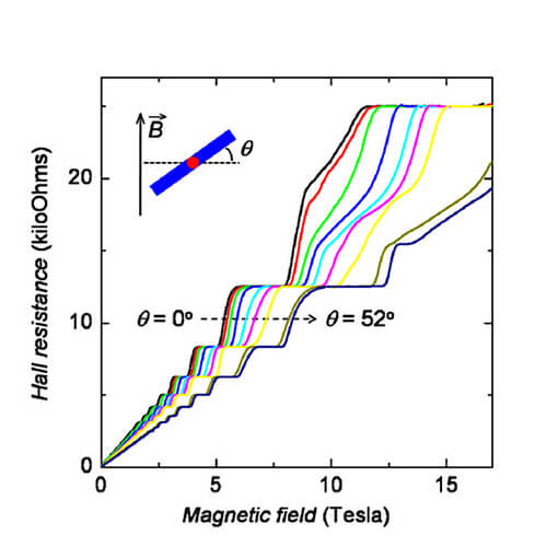
Orbital ferromagnetism in twisted bilayer graphene below 30 mK
Van der Waals heterostructures, particularly in the form of magic-angle twisted bilayer graphene (tBLG), are one of the hottest topics in today's solid state physics research. Previous measurements on tBLG already indicated ferromagnetism and Chern insulating behavior as deduced from a large hysteretic anomalous Hall effect which was subsequently confirmed to be quantized. A. L. Sharpe and co-workers now experimentally showed via transport measurements that the ferromagnetism in tBLG is highly anisotropic, strong evidence for an orbital rather than spin origin of ferromagnetism, something never before observed at low magnetic field.
For their measurements, the group mounted a sample of tBLG encapsulated in boron nitride flakes onto attocube's atto3DR double rotator, working at electron temperatures down to less than 30 mK facilitated by careful filtering, and in magnetic fields of up to 14 T. A dedicated in-situ calibration of the tilt angle using the Hall resistance allowed for accurate control of the exact in-plane and out-of-plane orientations during their experiments.
This measurement was realized with the atto3DR.
Further reading:
A. L. Sharpe et al., Nano Lett. 2021, 21, 10, 4299–4304
Rotating transport measurement setup at 25mK
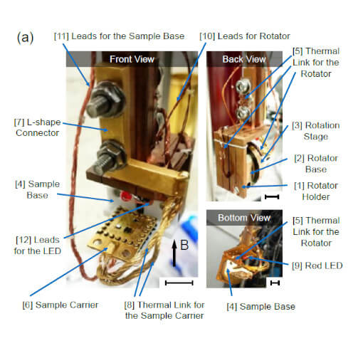
When designing a setup for mK applications material choice and thermalization is crucial. Titanium becomes superconducting at temperatures below 400 mK consequently, the thermal contact to the sample is not ensure anymore. At Peking University (Beijing, China), Dr. Pengjie Wang from Xi Lin group has chosen the beryllium-copper version of the ANR101 positioner with resistive readout to realize their low-electron-temperature sample rotation system for transport measurements inside a dilution cryostat. The rotator allows to orient the sample in-situ with respect to a high magnetic field of up to 10 T.
The dilution cryostat with a diameter of 81 mm offers the required space for the rotator setup, see picture. The sample holder is designed for the use of up to four sample, each 5 mm x 5 mm large, a red LED is installed to illuminate the samples at 4 K for an easier orientation. The measured electron temperature in the setup is 25 mK, the same as the environmental temperature.The setup is designed for transport measurements and material characterization at ultra-low electron temperatures. A first application shows the tilt-induced localization and delocalization of the second Landau level of the two-dimensional electron gas - an experiment for which a pressurized liquid ³He cell had been necessary elsewise.
(Figure reproduced from Rev. Sci. Instrum. 90, 023905 (2019); doi: 10.1063/1.5083994, with the permission of AIP Publishing)
This measurement was realized with the ANR101/RES/LT - rotator (360° endless).
Enhancing Quantum Dot Emitters by Precisely Positioned Micrometric SILs
Using interferometric closed loop scanning integrated into the attoCFM I confocal microscope for cryogenic in-situ lithography, the group of P. Michler in Stuttgart was able to optically localize quantum dots (QDs) with a unprecedented precision of 2 nm and mark them via lithography.
This procedure enables further processing and optimizing these single photon emitters to enhance light extraction. In this case, they successfully demonstrated how to precisely add hemispherical lenses directly on top of the quantum dot via 3D direct laser writing. This led to an enhancement in extraction efficiency by a factor of 2.
“Our attoCFM I LT-lithography setup is not only the best choice when it comes to stability requirements. Its closed loop scanning feature also allows us to optically pre-select quantum dots suitable for desired experiments and mark them in-situ via lithography with nanometric precision.”
Prof. Dr. Peter Michler (University of Stuttgart, Germany)
This measurement was realized with the attoCFM I, and the Low Temperature Photolithography.
Low temperature magnetization reversal properties of SrRuO3
Understanding the dynamics of magnetization reversal in materials is key to assessing their potential for magnetic storage. Most studies so far have concentrated on room temperature experiments. However, this only represents a narrow range of relevant parameters. L. Landau and co-workers from the group of Lior Klein (Bar-Ilan University, Ramat-Gan, Israel) explored the other end of the parameter range. Using the attoAFM I they studied the low temperature magnetization reversal properties of SrRuO3.
This measurement was realized with the attoAFM I.
Differential conductance measurements on Pd break-junctions measured
In this application, an attocube 4-point probe station is used to perform tunneling spectroscopy measurements in metallic nanogap devices at cryogenic temperatures. A single nanowire is contacted by two probes and a thermally-assisted electromigration process is employed to create a sub-nanometer tunneling gap.
Nanopositioners independently move each DC probe along the x, y, and z directions, enabling electrical contact to each device in succession. The contacting process is monitored by an inspection optics that provides good optical resolution to securely contact the pads of about 50 - 100 µm in size.
This measurement was realized with the Cryogenic Probe Station.
Angle-dependent transport measurements at 40 mK
Based on an attocube systems rotator ANR30/LT a rotation stage for angle-dependent transport measurements in magnetic fields up to 33 T and temperatures down to 40 mK was built at the user facility of the High Field Magnet Laboratory in Nijmegen.
The mixing chamber of the commercially available dilution refrigerator from Leiden Cryogenics offers only a limited space of 17 mm in diameter. Hence, the ultra compact attocube rotator ANR30/LT is the positioner of choice for this task. The rotator is fixed on a plastic (Hysol) dilution refrigerator insert.
This measurement was realized with the ANR31/LT rotator made from Titanium and CuBe.
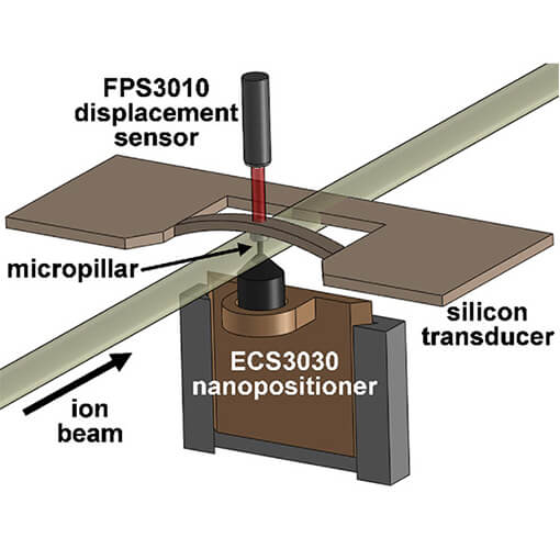
Measurements of Irradiation-Induced Creep
S. Özerinç and his colleagues at the University of Illinois at Urbana-Champaign have developed an apparatus for measuring irradiation induced damage and stress on the nanometer scale. Using attocube's ECS3030 as well as the FPS3010 interferometer, the system can measure in situ the deformation of mechanically stressed micro-pillars, during which the pillars are irradiated with heavy MeV ions. The apparatus provides a new and effective approach to accelerate the evaluation of promising materials for future nuclear power plant applications.
This measurement was realized with the ANPx101/RT - linear x-nanopositioner, and the Displacement Measuring Interferometer.
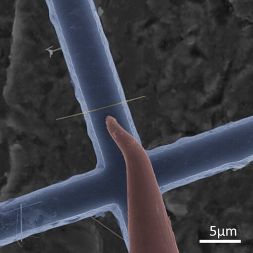
Mapping and Manipulation of Leakage Currents in a Nanostructure
In this application note, attocube’s smallest titanium positioners (ANPx51/RES and ANPz51/RES) are used as part of an atomic force microscope (AFM) inside a Janis ³He cryostat with a base temperature of 280 mK. The setup is a combined low temperature AFM and scanning tunneling microscope (STM), which is emploied to carry out scanning gate microscopy experiments on various nanostructures. In these measurements the positioners are used to move the metallic tip directly above the nanostructure predominantly at 4.2 K but also as low as 280 mK.
This measurement was realized with the ANPx101/RES/LT - linear x-nanopositioner, and the ANPz102/RES/LT - linear z-nanopositioner.
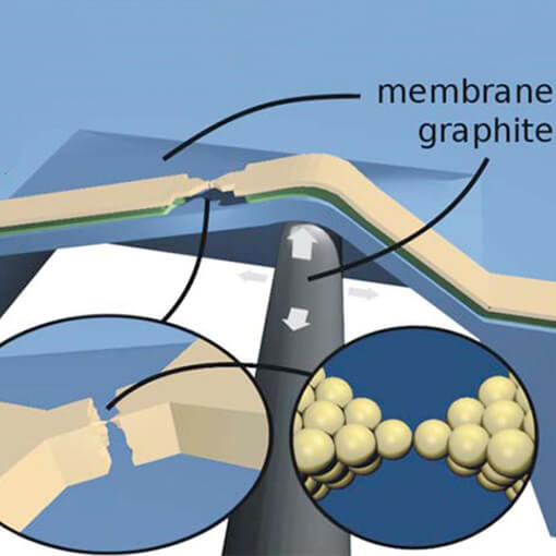
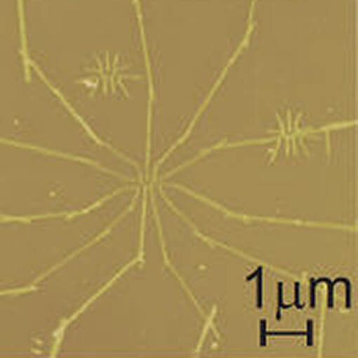
Mechanically Controlled Multi-Contact Break Junctions
In this application, small tips made from either glass or graphite were used to locally deform a silicon membrane, creating break junctions in a very controlled fashion. The tips with a typical radius between 50 and 200 microns were precisely controlled using attocube’s nanopositioning technology. The approach of locally creating and controlling individual break junctions can be used to study the influence of optical excitations on the conductance of individual molecules and for controllable metallic single-electron transistors.
This measurement was realized with the ANPx51/LT - linear x-nanopositioner.
Sample Nanomanipulation of 1-D Nanostructures
The group of Horacio Espinosa at Northwestern University has employed attocube‘s ECS3030 positioners (controlled by an ECC100 piezo-controller) to accomplish nanometer precise manipulation of various nanotubes inside a SEM chamber. Once a nanowire is picked up, the manipulator is used to position it on top of a MEMS device for testing elastic strength as well as for four-point electrical measurements.
This measurement was realized with the ECSx3030/StSt/HV.
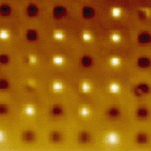
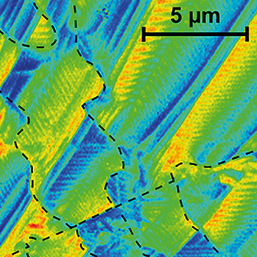
Ferroelectric Domain at Cryogenic Phase Transitions
Ferroelectric barium titanate (BTO) exhibits several ferroelectric phase transitions at cryogenic temperatures, resulting in severe structural changes and domain formation. Using an Attocube AFM I, the group of Prof. Eng (Institute of Applied Physics, Dresden University of Technology, Dresden, Germany) has investigated this domain dynamics in BTO single crystals applying both piezoresponse force microscopy (PFM) and Kelvin probe force microscopy (KPFM) down to 10 K. The two images display the PFM signal (a) and surface potential measured by KPFM (b) in contact and non-contact mode, respectively, over the same 15 µm x 15 µm sample area at T = 220 K (orthorhombic BTO phase).
This measurement was realized with the attoAFM I.
Performance Characterization of a Cryogenic Probe Station attoCPS I
In a series of tests with the attocube systems probestation, Munich researchers have found significant benefits for their research of nano-electro-mechanical structures and related high frequency experiments. In the basic version, the cryogenic probe station consists of four 3-axes positioning stacks (ANPxyz50/LT) allowing to position four probes independently onto a sample with high precision (max. sample diameter: 6 mm).
This measurement was realized with the Cryogenic Probe Station.
Magnetoresistance of self-assembled GaMnAs based nanowires
The relatively new class of self-assembled ferromagnetic nanowires could potentially be used for producing e.g. one-dimensional spin valve transistors or ferromagnetic single electron transistors, while maintaining a high flexibility in the choice of material as well as the axial and radial degrees of freedom. Due to the arbitrary orientation inherent to self-assembled materials on the substrate, typical characterization techniques such as magnetoresistance measurements conducted at cryogenic temperatures greatly benefit from the possibility to freely change the mutual orientation of external magnetic field and sample. To avoide an expensive 3D vector magnet the atto3DR, a 3-dimensional rotator offers a good a reliable solution for transport measurements which is in particular interesting in the field of mesoscopic physics at cryogenics.
This measurement was realized with the atto3DR.
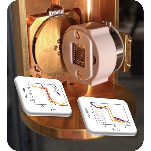
Van der Waals heterostructure under rotation at 40 mK
Understanding the mechanism of high temperature (high Tc) superconductivity is a central problem in condensed matter physics. Van der Waals heterostructures provide novel materials as model systems for quantum phenomena. An international collaboration (Berkeley, Stanford, Shanghai, Tsukuba, Seoul) reports in Nature signatures of tunable superconductivity in these special heterostructures, detected via a sharp drop in the resistivity and a plateau in the I-V curve below 1 K.
The transport measurements are performed in a dilution cryostat with a base temperature of 40 mK achieved through careful filtering. For in-plane measurements, the atto3DR double sample rotator was used, which conveniently allows for using the full field of a single solenoid in an arbitrary orientation. The authors find transitions from the candidate superconductor to Mott insulator and metallic phases, proving that the TLG/hBN superlattice provides a unique model system to study the triangular Hubbard model and its relation to unconventional superconductivity as well as potentially novel electronic states.
This measurement was realized with the atto3DR.
Further reading:
Guorui Chen, et al.; Nature, 572, 215–219 (2019)