

Surface Science
analysis of thin films & surfaces
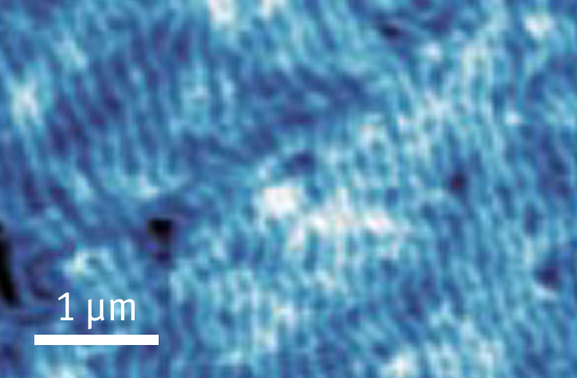
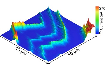
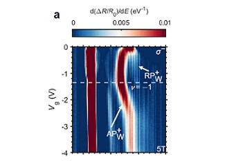
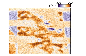
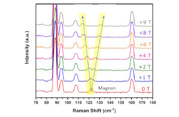
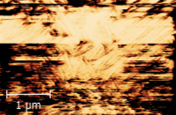
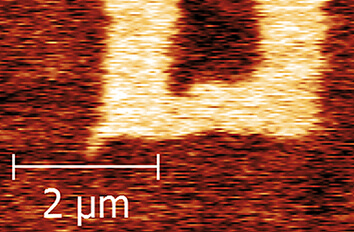
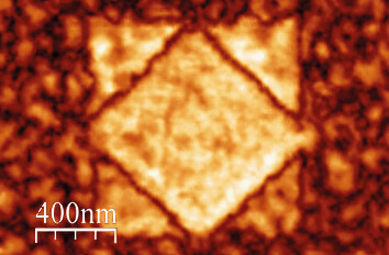
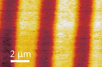
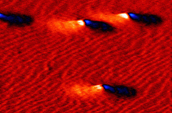
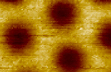
Surfaces of materials or thin films hold a complete micro cosmos of physical properties that are hot topics of today's research. The type of measurements to analyze the surface structure of magnetic materials, superconductors, graphene and 2D materials range from atomic force microscopy (AFM) to magnetic force microscopy (MFM) and to transport measurements. In addition, intrinsic properties and electronic structure such as vortex formation, the properties of topological insulators, multiferroics, ferroelectrics and domain walls are analyzed using low temperature Raman and electrical transport techniques as well as low temperature scanning microwave impedance microscopy (LT-sMIM).
Research Fields
- magnetic material properties
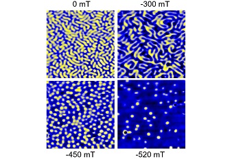
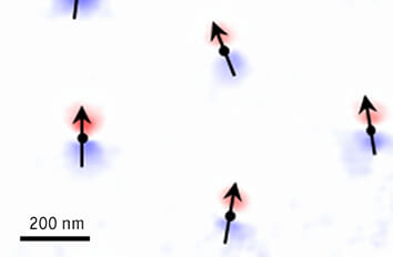
- magnetic imaging
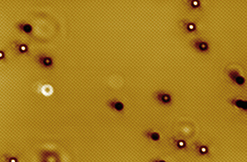
- superconductors & vortex imaging
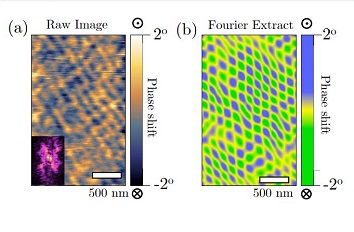
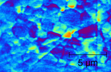
- electronic structure of sample surfaces
- surface polariton mapping
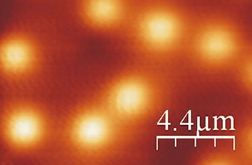
- graphene & 2D materials
- superconductor and semiconductor physics
- topological insulators
- stress / strain mapping
- ferroelectrics, multiferroics & domain walls
Application Snippets

Related Products
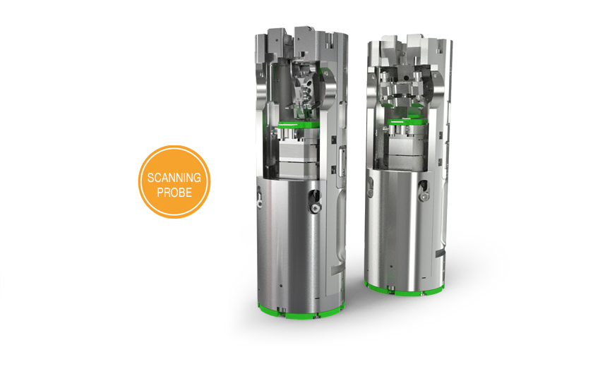
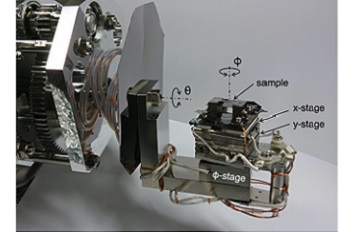
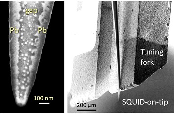
Scanning Probe Microscopes
With our scanning probe microscopes, attocube is the unchallenged industry leader in materials characterization on the nanoscale at low temperatures and in high magnetic fields.
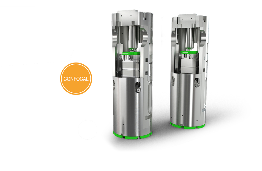
Confocal Microscope Platforms
With low temperature confocal microscopy, attocube has been pioneering the market for photoluminescence & spectroscopy on quantum dots and other single photon sources since its foundation.
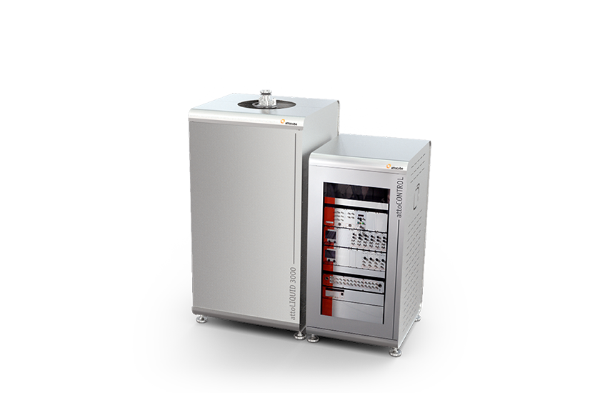
Liquid Helium Cryostats
The attoLIQUID helium-based cryostats feature variable temperature down to the mK range, large sample space, fast cooldown and ultra-low vibrations.
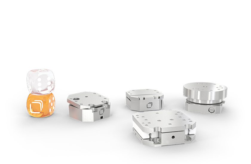
Low Temperature Nanopositioners
Cryogenic nanopositioners are designed for nanopositioning over millimeter ranges with the highest precision under extreme conditions such as cryogenic temperatures, high magnetic fields, and ultra high vacuum.
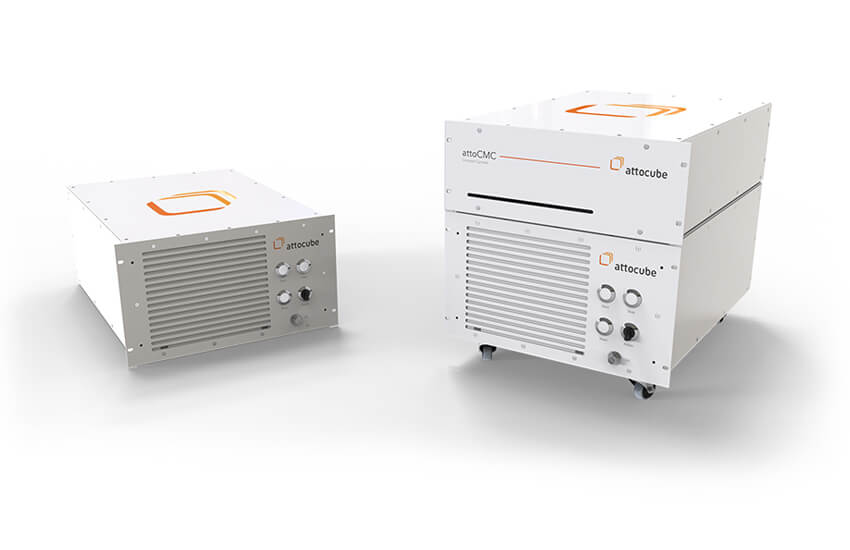
Compact Mobile Cryogenics
The CMC line offers infrastructure autonomy for sub-4K applications by combining a revolutionary compressor technology with high-performance cryogenic cooling systems.