

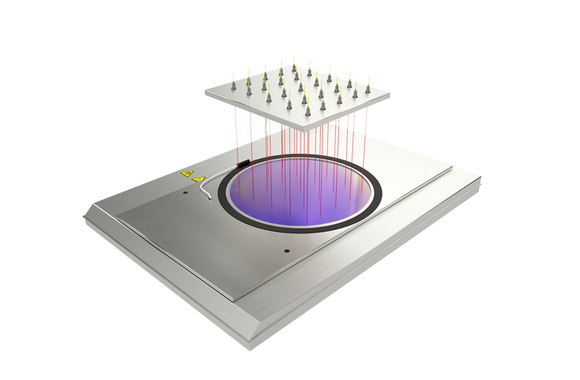
Planarity Detection
of wafers
During the lithography and metrology processes the wafer is exposed to extreme environments, fast motions and multi-dimensional forces. These could cause elastic or plastic deformation of the wafer which influences the wafers planarity. Uneven wafers reduce the accuracy of lithography processes and distract results of metrology analyses.
For example the movement of wafer stages working with magnetic levitation deforms in direction perpendicular to the flat surface of the plate. The operating status of the wafer stage motor influences the level of deformation. To optimize the operation mode of wafer stages and therefore reduce the wafer deformation during lithography process, a nanoprecise and contactless detection of wafer deformation is required.
attocube's solution
attocube´s interferometer sensor IDS3010 is capable of measuring directly on the wafer or on mirrors to capture deformations in nanometer range. The miniaturized design of the sensor heads allows to measure the deformation at several places on the same wafer to detect more-dimensional deformations. It can be used under extreme environmental conditions such as vacuum or other harsh environments.
Download the Application Note: Measuring the Deformation of a Magnetically Levitated Plate
Displacement Sensor IDS3010
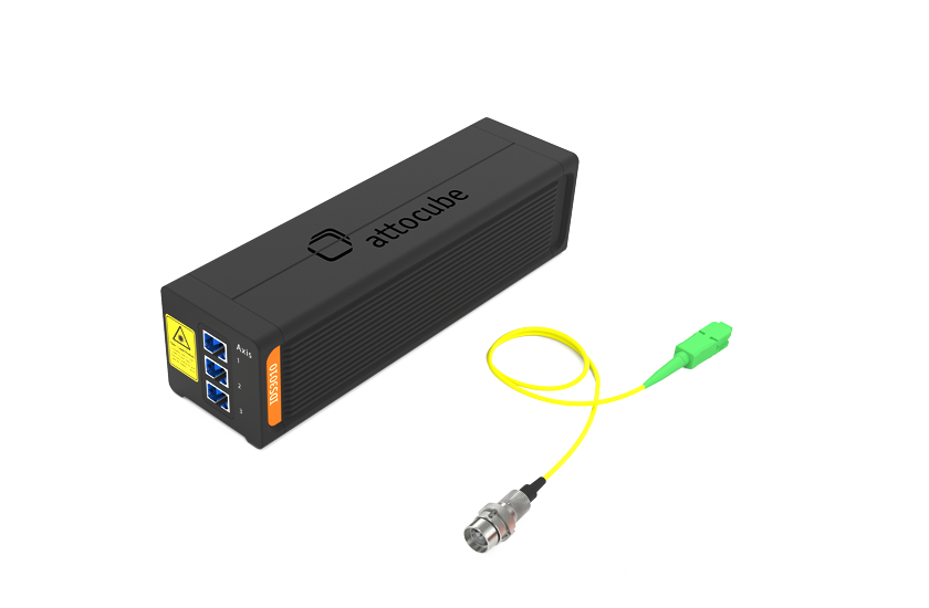
Control Unit
- multi-axis measurements
- certified accuracy in nanometer range
- 10 MHz measurement bandwidth
Sensor Heads
- vacuum compatible
- pluggable
- compatible to different surfaces (wafers, mirrors, polished metal…)