Wafer and Mask Inspection
quality assurance in wafer processing
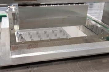
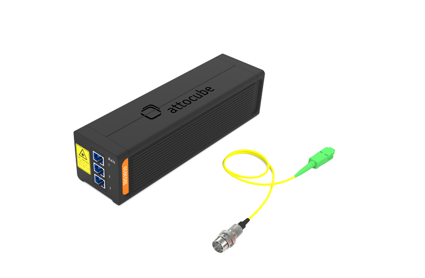
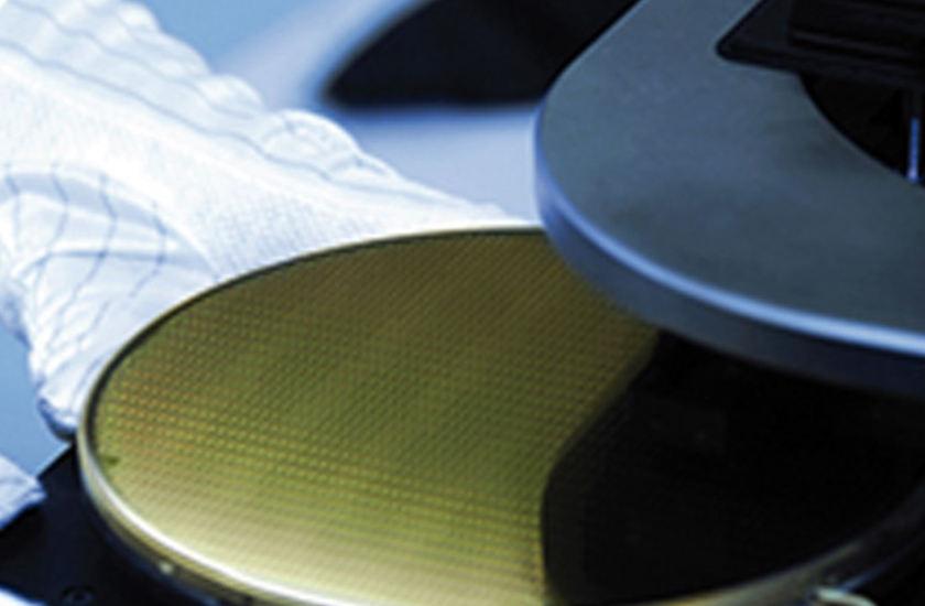
The miniaturization of printed-circuit boards (PCB) and microchips requires increasingly accurate sensors and actuators to be used in manufacturing and quality control processes of the semiconductor industry. The piezo-based nanopositioners are used for moving apertures or mirrors, e.g. for beam shaping. Wafers, wafer masks, and wafer chucks need highest motion accuracy that is easily fulfilled by attocube’s nanopositioners – even for individual applications. In photolithography, attocube's interferometers are used as the core component for metrology in quality control that directly measures on the optical material without making contact. Not only the wafer but also the quality of the mask can be detected using the interferometer as they are capable of performing noncontact measurements on glass and other optical materials. Both interferometers and nanopositioners can be used in a clean-room environment and they are compatible to harsh environments like high vacuum or high temperatures.