
Electron Beam Aperture Positioning
for microscopy and lithography tools
Electron-beam systems are used in a wide range of scientific and industrial applications. Specifically, in the semiconductor industry e-beam applications are common within lithography systems and microscopy tools for physical defect inspection.
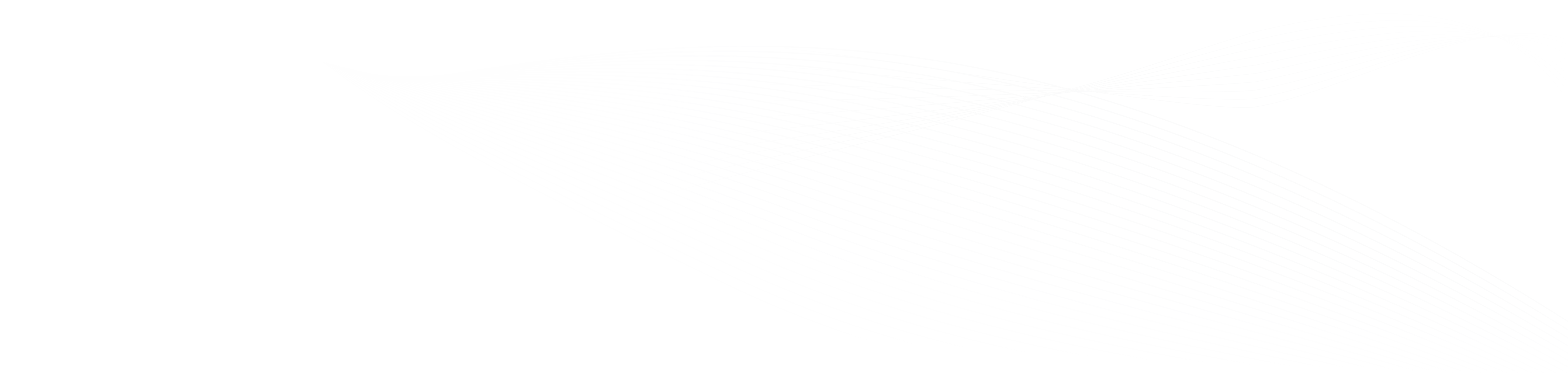
To this day, e-beam systems offer the highest resolution for the smallest structures, but are limited in regards of throughput. Multi stencil character projection can significantly increase the throughput. However, the increased complexity of such systems requires nano precise alignment of the components in ultra-high vacuum conditions and often at elevated temperatures.
attocube's solution
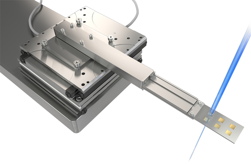
Besides highest precision, attocube’s nanopositioners fit well with the required harsh environments. The positioners are suitable for pressures down to 5 x 10-11 mbar, extreme temperatures and offer clean room compatibility. Furthermore, the compact design allows facilitated integration of single positioners or multi-axis motion systems.
Download the application note Accurate Electron-Beam Lithography and Microscopy
Nanopositioners
- nanometer precision
- UHV compatibility up to 5x10-11 mbar
- bake out up to 150° C