Light Controlling Materials
wave-attenuation, mode-profile & dispersion
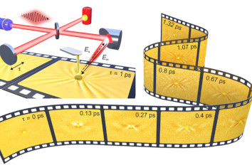
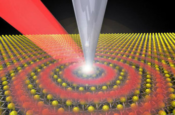
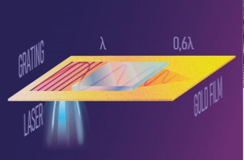
Light controlling nanomaterials refer to a class of materials that are engineered at the nanoscale to control the interaction of light with matter. These materials are designed to have unique optical properties that allow them to manipulate the behavior of light in various ways, such as absorbing, scattering, reflecting, or transmitting light.
These materials are being studied using neaspec technology for their potential applications in a wide range of fields, including optical communications, sensing, imaging, and energy conversion. To learn more about the recommended neaSCOPE microscope for these samples visit the product pages indicated below.
APPLY FOR A TEST MEASUREMENT ON YOUR SAMPLE*
* In order to evaluate the capabilities of our technology & products, you may apply for a test measurement with your own sample. Sucessful test results significantly increase the approval chance of your grant application.
Samples/Research Materials
Waveguides
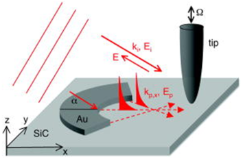
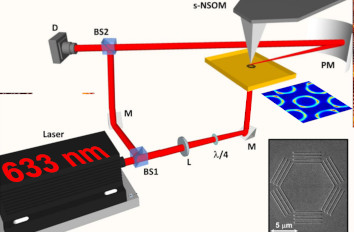
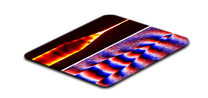
Optical waveguides are essential components in many optical systems, such as fiber optic communication networks, optical sensors, and photonic integrated circuits. They are used to transmit and manipulate light signals in a highly controlled and efficient manner, making them a critical technology in modern optics and photonics. For example, neaSCOPE is utilized in optical waveguides studies to advance integrated photonic circuits, which are analogous to electronic circuits but use light instead of electricity to transmit and process signals. Such circuits can be used in applications such as computing, sensing, and telecommunications.
Recommended product: VIS-neaSCOPE+s
Antenna
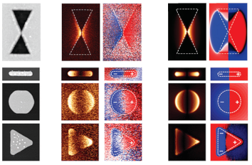
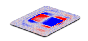
Nanoantennas work by concentrating and enhancing the electromagnetic field around the nanoparticle, which allows them to manipulate light in a highly controlled manner. The size and shape of the nanoantenna can be tuned to interact with specific wavelengths of light, which makes them useful for a variety of applications in optics and photonics. For instance, neaspec technologies allows our users to optimize optical data storage, by increasing the data density storage. In addition, neaSCOPE microscopes are used in plasmon-enhanced spectroscopy.
Recommended product: IR-neaSCOPE+s
Meta-Materials
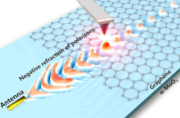
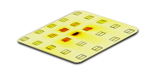
Nanometamaterials are engineered materials with unique optical, electrical, or magnetic properties adjustable by their nanoscale structure. The nanostructures in nanometamaterials can be designed to interact with electromagnetic radiation, such as visible light or infrared radiation, in specific ways and allows them to have a wide range of potential applications in several fields of study, e.g. photonics, energy, and sensing. As an example, neaSCOPE can be used to study metamaterials with negative refractive index, which is a material that bends light in the opposite direction to that in which it would normally bend in a natural material. This property allows negative refractive index materials to have potential applications in optical cloaking and imaging.
Recommended product: VIS-neaSCOPE+s
Plasmonics Structures
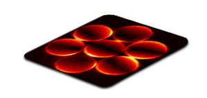
Plasmonic nanostructures are nanoscale structures made of metals designed to sustain surface plasmons. Surface plasmons are collective oscillations of the free electrons in the metal that can be excited by light, leading to strong interaction between light and matter at the nanoscale. One important application targeted by neaSCOPE users is single-molecule sensing by functionalizing the surface of the nanostructure with molecules.
Recommended product: VIS-neaSCOPE+s


