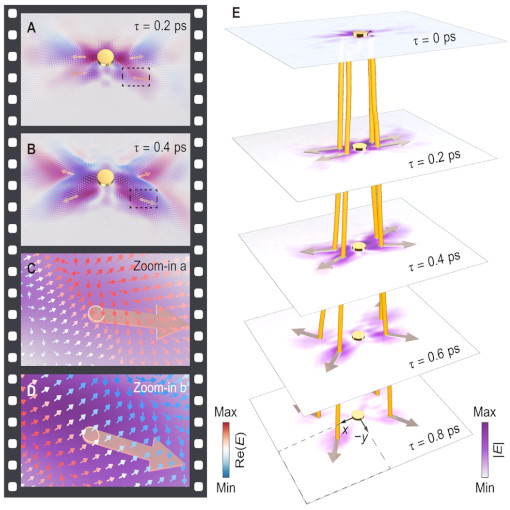
Unveiling Polariton Pulse Dynamics
This study explores polariton pulses - unique light-matter waves - and their complex behaviors in anisotropic media, driven by ultrafast and minuscule field changes. Using innovative time-resolved nanoimaging and advanced data processing, researchers have unveiled fascinating spatiotemporal dynamics, like curved energy flows and differing wave and energy velocities.The paper highlights the inadequacies of current technologies in capturing these rapid, directional, and nanoscale phenomena. The breakthrough nano-FTIR technology overcomes these limitations, enabling detailed visualization and analysis of polariton pulse behaviors. This advancement paves the way for transformative developments in ultrafast nanoimaging, with implications for molecular sensing, hyperlensing, and nanophotonic energy control.In summary, this research opens new horizons in optics and material science, from investigating intricate space-time dynamics at unprecedented scales to advancing ultrafast nanoimaging, marking a significant leap in the field.
This measurement was realized with the IR-neaSCOPE+fs.
Further reading:
Zhang et al., Science Advances 9, eadi4407 (2023)
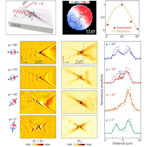
Polaritons Defy Symmetry
Nanoscale polaritons are crucial for nanophotonic devices. Hyperbolic polaritons (HPs) in high-symmetry crystals often lack directionality. In a recent eLight publication, scientists led by Profs. Zhang, Li, and Dai introduced a technique for anisotropic HP excitation and propagation. They discovered hyperbolic shear polaritons in low-symmetry crystals with enhanced directional propagation. This approach allows control of HPs' mirror symmetry without needing low crystalline symmetry. It enables tunable asymmetric polariton propagation, expanding possibilities for nanoscale light control and reconfigurable polaritonic devices.Introduced method breaks mirror symmetry in crystal polaritons, enabling control of asymmetry in HP responses. Offers nanoscale light manipulation and potential applications in nanoimaging, photonics, and quantum physics.
This measurement was realized with the IR-neaSCOPE+s.
Further reading:
Hu et al, eLight 3, 14 (2023)
SciTechDaily Article
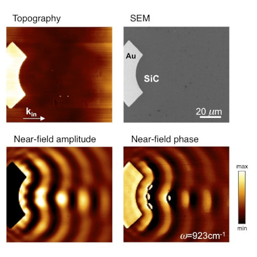
Optical Surface Waves
Infrared near-field microscopy allows to study the propagation of surface waves in the infrared spectral regime. Amplitude and phase resolved near-field images reveal local interference effects or enable the determination of the complex wave vector of surface waves. Surface waves can be excited in the mid-infrared spectral regime by e.g. metal structures on Silicon Carbide (SiC) crystals (propagating Surface Phonon Polaritons, SPhP). The topography image shows a circular structure used to excite SPhPs. The SPhPs propagate normal to the edge of the metal film and the curved structure leads to a focusing effect of the waves. The near-field amplitude image clearly reveals a locally enhanced signal about 40 µm away from the structure. Note that the metal structure is illuminated by a plane wave (used to excite the SPhPs) which interferes with the field of the surface waves. The images demonstrate that infrared near-field microscopy can be used for amplitude and phase resolved studies of e.g. spoof plasmons with tailored optical properties in detail.
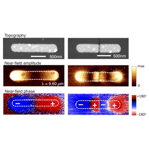
Analyzing Optical nano-Antennas
Near-field microscopy can be used to analyze the local field of photonic structures. Near-field images of a resonant (verified by far-field spectroscopy) antenna exhibit the clear signature of a dipolar oscillation mode on the Au rod. Note that the probing tip preferentially selects the z-component (normal to the sample surface) of the optical field. The amplitude image exhibits a high signal at the rod ends which are 180° out of phase. If the antenna structure is modified by e.g. a cut at the centre of the Au rod (fabricated by FIB), the near-field images reveal two dipolar oscillation modes on the segments. Systematic studies allow to analyze the coupling between the segments and to characterize the optical properties of the antenna structures. Polarized measurements allow to filter out specific components of the optical field associated to photonic structures or devices and to investigate the field e.g. in the antenna gap.
This measurement was realized with the VIS-neaSCOPE+s.
Nanoscale Negative Refraction
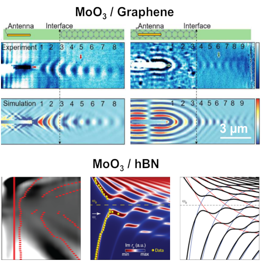
Refraction is a familiar effect in which a light beam alters direction as it propagates from one medium to another. Negative refraction is a nonintuitive but well-established effect in which the light beam is bent in the “wrong” direction. Two groups now independently demonstrate negative refraction at the interface of two-dimensional van der Waal materials. Hu et al. used molybdenum trioxide with a graphene MoO3 / Graphene overlayer to show that in-plane negative refraction of mid-infrared (mid-IR) polaritons occurs at the interface and is gate tunable. Sternbach et al. used molybdenum trioxide/hexagonal boron nitride MoO3 / hBN bicrystals to show that negative refraction of mid-IR polaritons occurs for propagation normal to the interface.
Polaritonic negative refraction in the mid-IR provides opportunities for optical and thermal applications such as IR super-resolution imaging, nanoscale thermal manipulation, and chemical sensing devices with enhanced sensitivity.
This measurement was realized with the IR-neaSCOPE+s.
Luttinger-liquid Plasmons
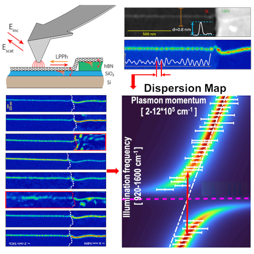
1D Luttinger-liquid plasmons formed inside carbon nanotubes (CNTs) are long-lived excitations with extreme electromagnetic field confinement. In the past, s-SNOM amplitude studies were limited to semiconducting CNTs which require additional doping. This s-SNOM phase study, allows investigation of metallic carbon nanotubes as they support strong tip-launched Luttinger-liquid plasmons at ambient conditions. The Authors extracted the dispersion relation of the hybrid Luttinger-liquid plasmon–phonon polaritons. The dispersion shows pronounced mode splitting, and an ultrastrong coupling regime with phonons of both investigated substrates, i.e., native silica and hBN. Such strong coupling of quasiparticles allows now applications like induced transparency, polariton lasing, changing of the rate of chemical reactions, or enhanced sensitivity in infrared and Raman spectroscopy
s-SNOM studies of Luttinger-liquid plasmons is an essential application to develop novel low-loss plasmonic circuits for the sub-wavelength manipulation of light.
This measurement was realized with the IR-neaSCOPE+s.
Further reading:
Németh et al., Nano Lett. 22, 3495 (2022)
Exciton-Polaritons Propagation
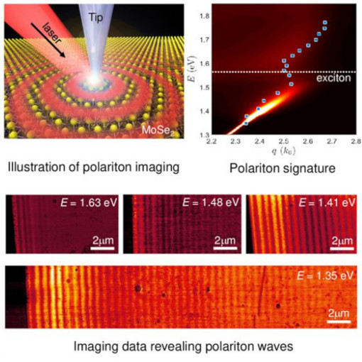
The exciton–polariton (EP), a half-light and half-matter quasiparticle, is potentially an important element for future photonic and quantum technologies. It provides both strong light–matter interactions and long-distance propagation that is necessary for applications associated with energy or information transfer. Recently, strongly coupled cavity EPs at room temperature have been demonstrated in van der Waals materials due to their strongly bound excitons. Here, we report a nano-optical imaging study of waveguide EPs in MoSe2, a prototypical van der Waals semiconductor. The measured propagation length of the EPs is sensitive to the excitation photon energy and reaches over 12 µm. The polariton wavelength can be conveniently altered from 600 nm down to 300 nm by controlling the waveguide thickness. Furthermore, we found an intriguing back-bending polariton dispersion close to the exciton resonance. The observed EPs in van der Waals semiconductors could be useful in future nanophotonic circuits operating in the near-infrared to visible spectral regions.
This measurement was realized with the VIS-neaSCOPE+s.
Further reading:
Nanowerk News
Hu et al., Nature Photonics 11, 356 (2017)
Plasmon nanojet-based superlens
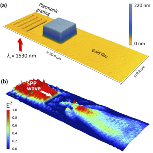
When a laser pulse of wavelength λ shines on the diffraction grating in the gold film, this gives rise to another type of electromagnetic excitations, known as surface plasmon polaritons. They propagate along the gold film and undergo 60% compression to a wavelength of 0.6λ when passing the square nanoparticle. This so-called plasmon nanojet effect, observed in the study for the first time, offers intriguing prospects for localizing light to the point where it becomes feasible to use it in fast and compact optical computers.
The authors proposed in this study a microstructure based on a dielectric cuboid placed on a thin metal film that can act as an efficient plasmonic lens allowing the focusing of surface plasmons at the subwavelength scale. Using numerical simulations of surface plasmon polariton (SPP) field intensity distributions, we observe high-intensity subwavelength spots and formation of the plasmonic nanojet (PJ) at the telecommunication wavelength of 1530 nm. The fabricated microstructure was characterized using amplitude and phase-resolved scattering-type scanning near-field optical microscopy. We show the first experimental observation of the PJ effect for the SPP waves. Such a novel, to the best of our knowledge, and simple platform can provide new pathways for plasmonics, high-resolution imaging, and biophotonics, as well as optical data storage.
This measurement was realized with the VIS-neaSCOPE+s.
Further reading:
News SciTechDaily
Minin et al., Optics Letters 45, 3244 (2020)
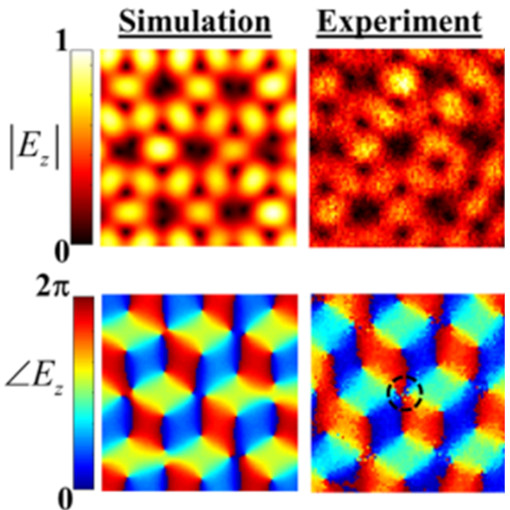
Optical Skyrmions
Best thought of as topological excitations that share the same topology as a set of magnetic moments wrapped around a sphere, skyrmions are widely thought to be promising for magnetic storage and spintronics applications. Shai Tsesses and colleagues have now brought skyrmions into the arena of optics. By controlling the interference of plasmon polaritons on a patterned metallic surface, they have succeeded in creating a lattice of optical skyrmions. The authors were able to image this pattern of evanescent electromagnetic fields using a phase-resolved near-field optical microscope. In contrast to their magnetic analogues studied in solid-state systems, these optical skyrmions can be continuously tuned from a so-called bubble- to Néel-type structure. However, in common with many such topological excitations, the lattice of optical skyrmions displays a remarkable robustness to imperfections.
The extent to which light can be manipulated and processed in photonic systems has already given us countess technologies. Few would bet against a few more popping out following this discovery of photonic skyrmions.
This measurement was realized with the VIS-neaSCOPE+s.


