
Ultra Precise Position Tracking
in photolithography
During the photolithography process circuit patters of few nanometers in size are transferred from the photomask (reticle) via various lenses onto the semiconductor wafer. After the photomask pattern is projected to one part of the wafer, the wafer stage is moved and the lithography process is repeated until the whole wafer is covered with the respective patterns.
The ultraprecise position tracking and alignment of measurement frame, optics and wafer stage is key condition to ensure highest quality throughout the lithography process. All components used in this process need to meet the requirements of clean room conditions and - depending on the technology - be capable to perform under vacuum and high temperature environments.
attocube's solution
attocube´s interferometer sensor IDS3010 with vacuum and high temperature compatible sensor heads can be easily integrated into lithography machines, ensuring the best alignment among the key components with nanometer accuracy, delivering high speed data with up to 10 MHz bandwidth.
Displacement Sensor IDS3010
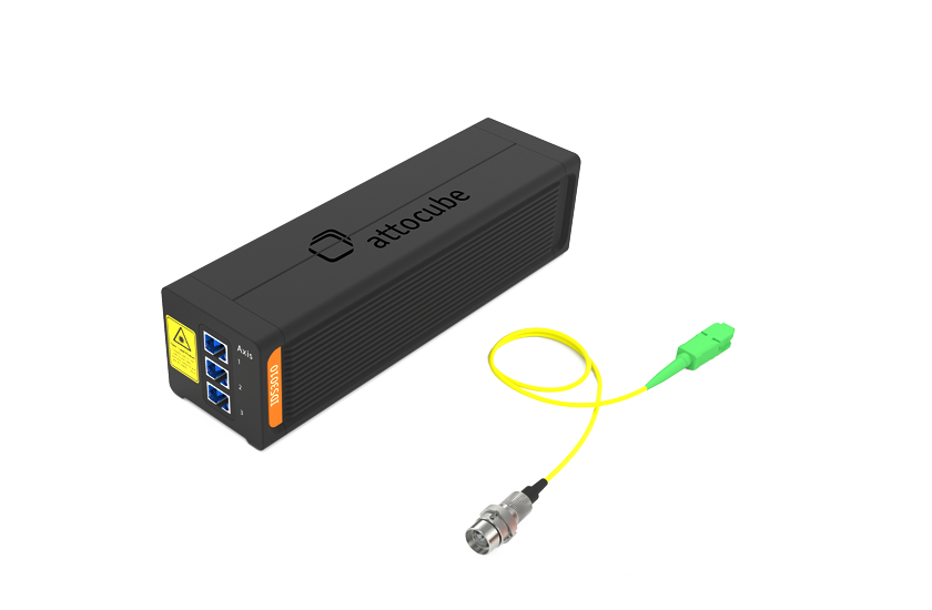
Control Unit
- 10 MHz bandwidth
- 2 m/s target velocity
- real-time
Sensor Heads
- vacuum compatible
- pluggable
- compatible with different targets