

Cryogenic Probing of PICs
photonic integrated circuits testing & device characterization
In the international research community, there is a clear trend towards on-chip photonic integrated circuits (PICs), with the clearly articulated goal to industrialize the technology. The vision is to develop industry-level photonic chips with extensive optical circuitry to carry out classical logical or quantum operations with many optical signals coupled in and out of the chip via several optical ports. In addition, electrical DC and HF signal control requires an elaborate electronic infrastructure.
The combination of photonic integrated circuits (PICs) and quantum technologies is a promising approach to significantly scale up optical quantum computing, as existing infrastructure of semiconductor manufacturing can be utilized. Similar to the classical fabrication process, frequent testing by wafer probers is crucial to ensure the required performance.
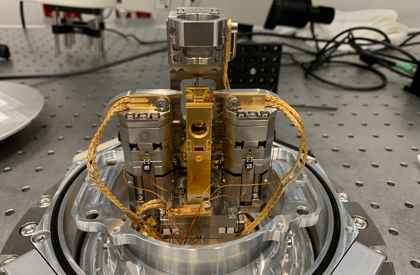
As PICs for quantum computing operate in cryogenic environments, new technology is needed to establish combined optical and electrical probe stations which are able to analyze these complex devices.
attocube's solution
attocube´s low temperature positioners are perfectly suited to individually position multiple optical fiber or electrical probes, as well as fiber arrays in cryogenic environments. Challenges like high precision movements, low heat dissipation, and stable position at the target location are met with attocube nanopositioners.
Despite their small size, designed to fit typical cryostat spaces, they offer travel ranges in the cm regime with nanometer precision. Thanks to the modular design, multiple degrees of freedom can be achieved in systems tailor made for the customer’s application.
Cryogenic Nanopositioners
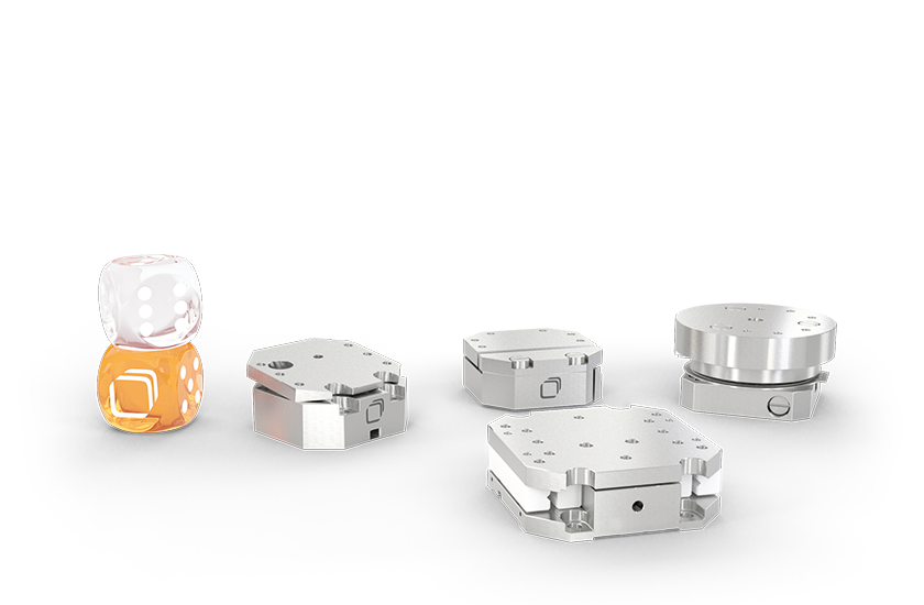
- down to milli-Kelvin
- multi-axis operation & modular design
- closed loop control
- large travel ranges