

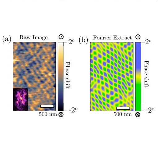
Conducting domain walls in quantum materials
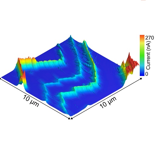
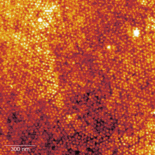
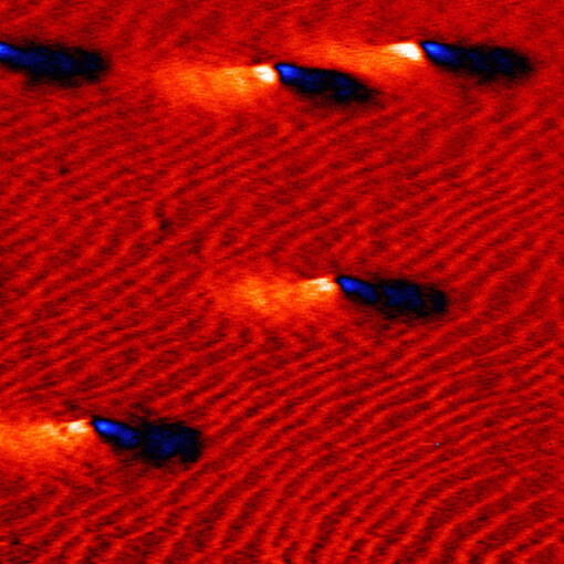
Conducting domain walls (DWs) are quasi-2D conducting pathways that can be created, positioned, and removed in-situ, giving an opportunity for rewritable nanoelectronics. In this young field, conducting DWs typically arise in wide band-gap ferroelectrics where they can form in response to charge build up at polar discontinuities. The chair of István Kézsmárki (University of Augsburg, Germany) has shown that conducting DWs can also exist in narrow-gap Mott insulators. In this case, it was shown that the nanoscale conducting pathways form because of strain gradients around the DWs that change the band structure.
The team used an attoAFM I microscope with a ct-AFM upgrade and a PFM upgrade in an attoLIQUID2000 cryostat to cool their template material (GaV4S8) below its Jahn-Teller transition (~43 K) before directly imaging the conductivity, the topography, and the piezoresponse. From this they were able to rule out the polar discontinuity model as the origin, rather correlating the increase in conductivity around the DWs to the square of height of the surface reconstruction: a signature of the volume strain that arises across the Jahn-Teller transitions. Effectively, this shows a new mechanism for creating nanoscale conducting pathways using strain-gradient-induced changes in band structure. This opens the exciting door for many new materials to be considered for domain wall nanoelectronics.
This measurement was realized with the attoAFM I.
Further reading:
L. Puntigam et al., Adv. Electron. Mater. 2022, 2200366 (2022)
Exciton-polarons optical fingerprint in moiré superlattice
Two-dimensional moiré materials provide a highly tuneable platform to investigate strongly correlated electronic states. Such emergent many-body phenomena can be optically probed in moiré systems created by stacking two layers of transition metal dichalcogenide semiconductors: optically injected excitons can interact with itinerant carriers occupying narrow moiré bands to form exciton-polarons sensitive to strong correlations. Here, the group of Brian Gerardot (Heriot-Watt University, UK) investigates the behaviour of excitons dressed by a Fermi sea localised by the moiré superlattice. Using temperature dependent magneto-optical spectroscopy with attoDRY1000, they identify the nature of exciton-polarons in the presence of strongly correlated electronic states and reveal the rich potential of theu MoSe2/WSe2 platform for investigations of Fermi–Hubbard and Bose–Hubbard physics.
This measurement was realized with the attoDRY1000.
Further reading:
Campbell, A.J. et al., npj 2D Mater Appl 6, 79 (2022)
Moiré Chern insulator for magnetic memories
In spin torque-based magnetic memories, magnetic bits can be switched using electrically-driven spin currents. The team lead by Andrea Young (University of California at Santa Barbara, USA) in collaboration with the group of Kin Fai Mak and Jie Shan (Cornell University, USA) has studied AB-stacked MoTe2/WSe2. This intriguing system showcases a remarkable accumulation of strong Berry curvature (BC) near the edges of the Hubbard band, resulting in a ubiquitous Spin Hall effect and a well-formed Chern insulator state at half filling of the moiré unit cell. Employing a nanoSQUID setup equipped with attocube nanopositioners (ANPx101, ANPz102) and scanners (ANSxy100), the team directly imaged the interplay between these two effects manifesting in ultra-low current magnetization switching within a singular system - a highly sought-after capability for efficient magnetic memory bits.
This measurement was realized with the ANPx101/RES/LT/HV - linear x-nanopositioner, and the ANPz101/RES/LT/HV - linear z-nanopositioner.
Further reading:
C. L. Tschirhart et al., Nature Physics 19, 807 (2023)
Mastering quantum computing via magnetic imaging with quantum probes
One of the most promising realizations of quantum computer relies on circuits of superconducting qubits. In order to come up with the optimal design of such circuits, physicists need to trace the paths of electrical currents. This can be done through monitoring the magnetic fields produced by the currents according to the Ampère´s law.
The team lead by Martino Poggio (University of Basel & Swiss Nanoscience Institute, Switzerland), in collaboration with the group of Andreas Wallraff (ETH Zurich, Switzerland), has imaged magnetic fields of a superconducting qubit circuit by scanning microscopy utilizing SQUID-on-tip (SOT) as the probe. In their experimental setup they used attocube cryogenic nanopositioners (ANPx311/LT/HV) and scanners (ANSxy100lr/LT/HV) at 4 K. Their method precisely detects both positive and negative effects of qubit couplings, making it instrumental in designing circuits with low qubit decoherence, which is a prerequisite for increased quantum computing efficiency.
This measurement was realized with the ANSxy100lr/LT/HV xy-Scanner made from Titanium, and the ANPx311/LT/HV - linear x-nanopositioner.
Further reading:
E. Marchiori et al., Appl. Phys. Lett. 121, 052601 (2022)
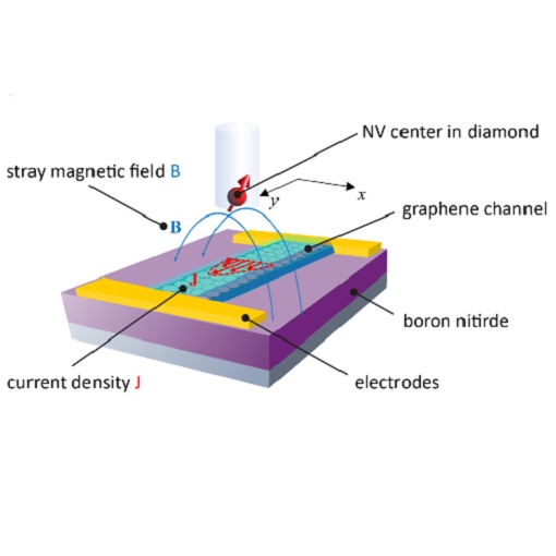
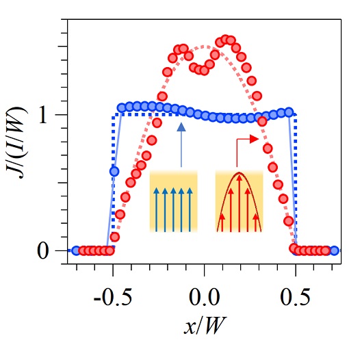
Viscous Dirac fluid paparazzied by NV magnetometry
Electronic transport in strongly-correlated quantum materials can involve substantial complexity that defy conventional description. An example of novel transport phenomenon that can arise in quantum materials is the collective movement of electrons reminiscent of that of a hydrodynamic fluid, in which viscosity can lead to non-uniform, parabolic current profile known as Poiseiulle flow. The electron-hole plasma in graphene at the charge neutrality point, known as the Dirac fluid, has been theoretically predicted as a candidate for such behavior. The team lead by Ronald Walsworth (prev. Harvard University, USA, now University of Maryland, USA) and Amir Yacoby (Harvard University, USA) established the existence of viscous Dirac-fluid flow in graphene by imaging the magnetic stray field associated with the electron flow. Imaging has been conducted by nitrogen vacancy magnetometry (NVM) in a setup comprising attocube nanopositioners ANP101 and ANS100. Single-spin scanning NVM, complemented by wide-field NVM imaging, reveals a parabolic Poiseuille profile, which is a characteristic of viscous transport, and in contrast with the uniform flow profile of conventional Ohmic conductors. Their results render NVM a suitable tool for probing the behavior of correlated electrons at the nanoscale.
This measurement was realized with the ANSxyz100std/LT xyz-Scanner made from Titanium, and the ANPx101/RES/LT/HV - linear x-nanopositioner.
Further reading:
M.J.H. Ku et al., Nature 583, 537 (2020)
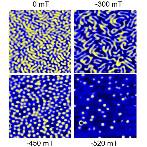
Constituents of racetrack memory devices
The quest for next-generation energy-efficient and ultra-high-density spintronic devices has been driving extensive research of magnetic skyrmions and antiskyrmions. These topologically protected non-collinear magnetic domain walls are promising candidates for carrying information in racetrack memory devices. The group of Stuart Parkin (Max Planck Institute for Microstructure Physics, Germany) has been leading the research in that direction, utilizing an attoAFM I microscope with an attoMFM upgrade in an attoLIQUID2000 cryostat. Below we summarize some of their recent results.
In a Heusler compound Mn1.4PtSn they found the size of antiskyrmions to be tunable by means of varying the thickness of the hosting single-crystal lamella, which was ascribed to the influence of magnetic dipolar interactions. Study of another Heusler compound, Mn2RhSn, reveals spin textures stabile over a wide range of temperature and magnetic field, similarly to the aforementioned single-crystalline case. Interestingly, creation and annihilation of these spin textures can be achieved with local magnetic field emanating from the magnetic tip of the cantilever, which opens the way towards skyrmionic devices base on Heusler thin films. Furthermore, they discovered that the size of Néel skyrmions in 2D layered ferromagnet Fe3GeTe2 is also proportional to the lamella thickness, and that the Dzyaloshinskii–Moriya Interaction therein is driven by the asymmetric distribution of Fe vacancies.
This measurement was realized with the attoAFM I.
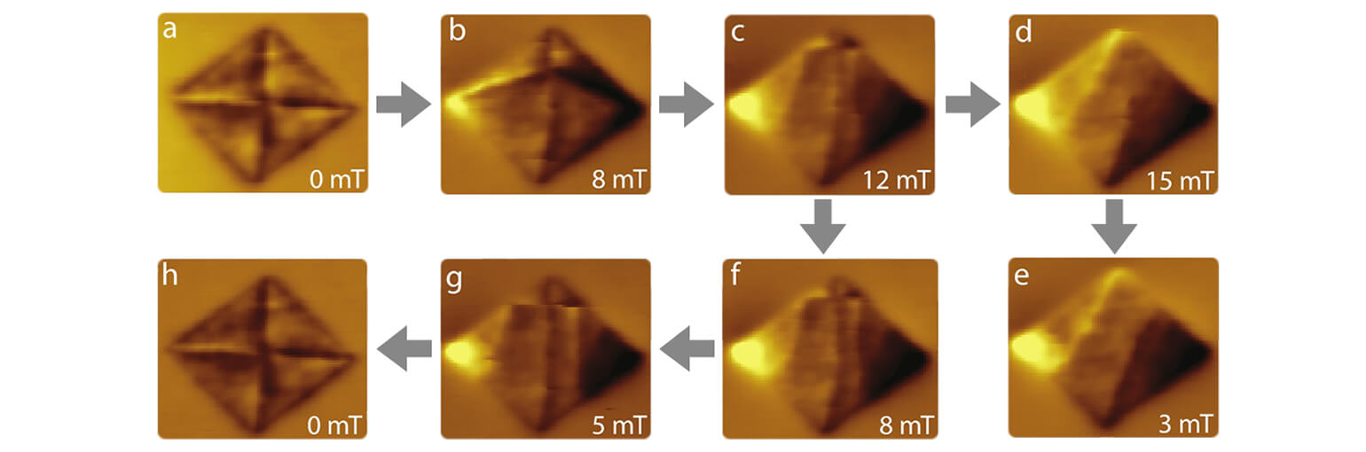
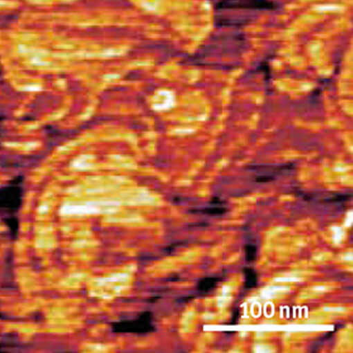
Zooming into heterochiral magnets
Topological spin textures have been in focus of nanoscience for years due to their applications potential in novel generation of spintronic devices. Yet, almost all effort has been dedicated to the study of homochiral states. Hence, little is known about long-range interactions between domains of opposite handedness, as well as how magnetic states are affected by high density of chiral domains and domain walls. The group of Sang-Wook Cheong (Rutgers University, USA) explored a layered chiral helimagnet Cr1/3TaS2 with tunable topological heterochiral states. By tuning the density of chiral domains, which can be achieved by varying the cooling rate at the phase transition, they observe inside each domain a topological magnetic texture in the form of a spiral composed of quasiperiodic Néel walls. Weak in-plane magnetic fields turn this spiral superstructure into a non-spiral array of concentric ring domains. These results have been achieved by utilizing an attoAFM I with attoMFM upgrade in an attoLIQUID2000 cryostat. The authors assign the existence of magnetic spirals to intrinsic strain present in the heterochiral state, which renders layered heterochiral materials interesting for applications in strain-tunable magnetic devices.
This measurement was realized with the attoAFM I.
Further reading:
K. Du et al., PNAS 118, e2023337118 (2021)
Skyrmions induced by strain gradient
Dzyaloshinskii-Moriya interaction (DMI) arises from breaking the inversion symmetry in noncentrosymmetric crystals, or emerges at thin-film interfaces. DMI and its relation to magnetic anisotropy are decisive in creating conditions for creation of chiral spin structures. The group of Prof. Jinxing Zhang (Beijing Normal University, China) has shown how DMI can be generated in a centrosymmetric material La0.67Sr0.33MnO3 by a strain gradient. Such DMI induces topological spin textures (skyrmions and spin spirals) accompanied by topological Hall effect in the range from 20 - 300 K. They imaged skyrmions and spin spirals by magnetic force microscopy (MFM) utilizing an attoAFM I microscope with attoMFM upgrade in an attoDRY1000 cryostat. Their findings open the path to exploring the potential for centrosymmetric magnetic materials in spintronics applications.
This measurement was realized with the attoDRY1000, and the attoAFM I.
Further reading:
Y. Zhang et al., PRL 127, 117204 (2021)
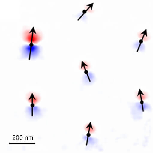
Ferroelectrically induced magnetic spin crystal
Whether the presence of skyrmions is the underlying cause for the topological Hall effect (THE) observed in SrRuO3 (SRO) heterostructures, is a matter of dispute, as conflicting experimental evidences exist. Samuel Seddon (Group of Marin Alexe, University of Warwick, UK) has conducted a series of magnetic force microscopy (MFM) measurements on a ferroelectric-SRO bilayer. These show that the breaking of inversion symmetry at the interface, induced by the strong polarization in the ferroelectric layer, does not induce skyrmions but rather an incommensurate spin crystal, that exists over the field range of THE. For the magnetic force microscopy (MFM) measurements they have been utilizing an attoAFM I microscope with attoMFM upgrade in an attoLIQUID2000 cryostat. Their findings exemplify that complex oxides host extremely reach physics, many aspects of which are yet to be unraveled.
This measurement was realized with the attoAFM I.
Further reading:
S.D. Seddon et al., Nature Commun. 12, 2007 (2021)
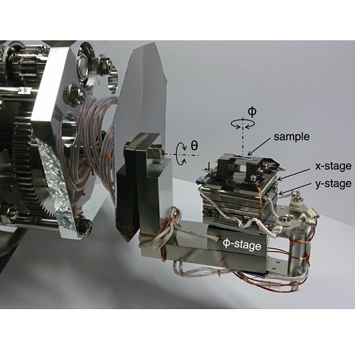
3D micro-structure sample positioning in 4 dimensions in a µ-RHEED/SEM system
Sohei Nakatsuka et. al from Tohoku University and Osaka University, Japan have designed a system for analysing a 3D micro-shaped structure on a Si substrate. Their system combines a micro-beam reflection high-energy electron diffraction (µ-RHEED) and scanning electron microscopy (SEM). Sample Manipulation is done in four dimensions via a mechanical rotation stage for glancing angle (Θ) and a 3D nanopositioner stack mounted onto the mechanical device. The 3D stack consists of two attocube ECSx3030 for xy-movement and one ECR3030 for azimuth angle (Φ) rotation. The sample manipulator enables precise positioning and rotation of the 3D microstructured sample to identify surface structures like surface morphology, surface orientation defined by Miller index, surface ordering, and surface reconstructed structures. attocube EC* series stages are the perfect fit due to highest precision within extrem environments like ultra-high vacuum and harsh radiation.
This measurement was realized with the ECSx3030/StSt/NUM+/HV.
Further reading:
e-J. Surf. Sci. Nanotechnol. 19, 13-19 (2021)
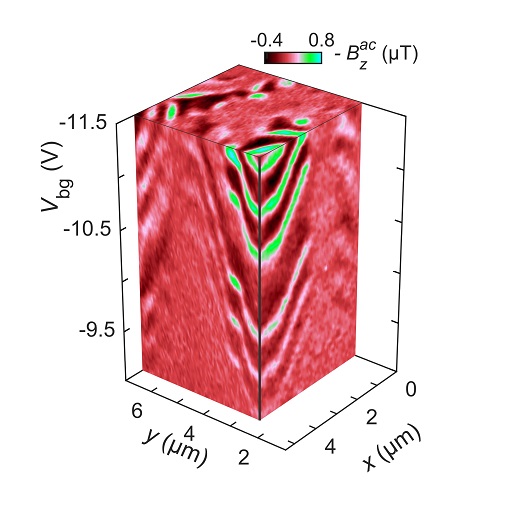
Tomographic magnetic imaging of Landau levels and twist-angle disorder in magic-angle graphene
Electronic correlations in magic-angle twisted bilayer graphene (MATBG) strongly depend on the interlayer twist angle Θ. MATBG bears potential of application in electronic devices, so it is crucial to understand the implications of local variations of Θ, as those could compromise the stability of competing orders in MATBG, as well as alter the phase diagram of the correlated states.
The group of Eli Zeldov (Weizmann Institute of Science, Israel) has achieved a breakthrough in mapping local variations of Θ utilizing scanning nanomicroscopy with SQUID-on-tip. They have established a correlation between local variations of Θ and transport properties of MATBG in the quantum-Hall-state regime, with unprecedented precision and spatial resolution. Their home-built experimental apparatus contains attocube low-temperature nanopositioners and an ASC500 scan controller.
This measurement was realized with the ASC500 Full Version.
Further reading:
A. Uri et al., Nature 581, 47 (2020)
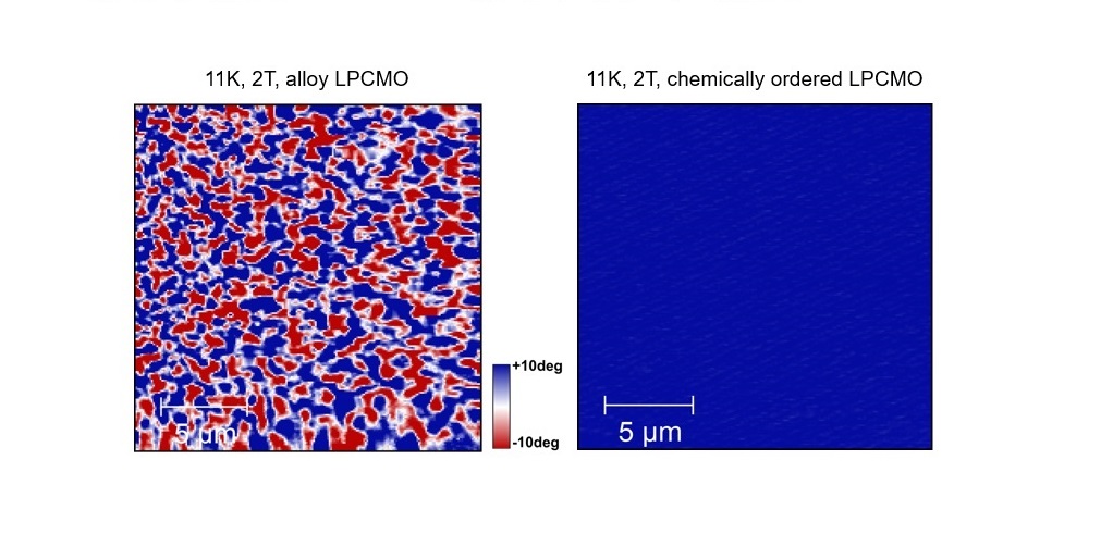
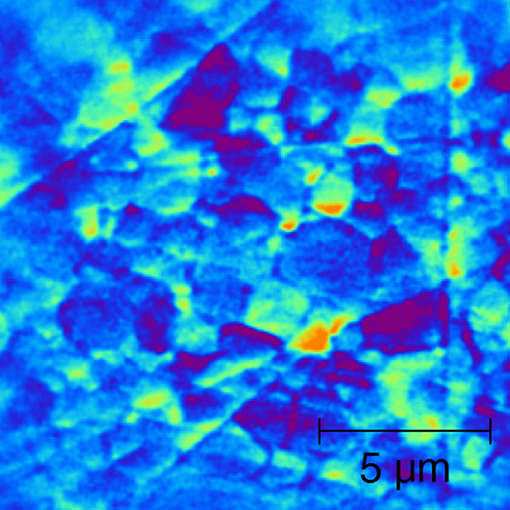
Revealing physical origin of electronic phase separation in complex oxides
Manganites exhibit various nonlinear responses to external stimuli, which makes them potentially useful materials for electronic devices. While nonlinear responses in complex oxides have been correlated to large-scale electronic phase separation (EPS), the physical origin of EPS has for a long time remained puzzling. The group of Jian Shen (Fudan University, China) has provided the first experimental evidence that the disorder induced by chemical doping is a prerequisite for EPS, thus verifying the theoretical predicition.
This result has been directly obtained by comparative MFM measuerments on chemically ordered manganite film vs. the chemically disordered one, utilizing an attoAFM I with attoMFM upgrade in an attoDRY1000 cryostat. Their finding opens the path to focused design of complex oxides with desired properties for applications, especially those exhibiting colossal magnetoresistance.
This measurement was realized with the attoDRY1000, and the attoAFM I.
Further reading:
T. Miao et al., PNAS 117, 7090 (2020)
Combined Laser Beam Epitaxy and Low-Temperature STM using ANPx321 Positioners
Adding new functionalities to an STM is a demanding task due to the strict requirements to the operating condition. On the other hand, being able to deposit material while using an STM enables to synthesize new material or characterize it more efficiently, because it frees from the need to interact with the sample.
The group of Prof. Qing Huan (Chinese Academy of Science, Beijing) has achieved such a feat by combining laser molecular beam epitaxy and a cryogenic STM. The STM operates at 5 K in ultra-high vacuum conditions and offers a sample-moving range of 15 x 15 mm2. The integrated ANPx321 positioners (closed-loop configuration) feature a positioning accuracy better than 1 µm. The multi-use STM demonstrates its performance by growing and analyzing various materials. Overall, the group expects to have provided a platform suitable for systematic research on new materials, including superconductors.
This measurement was realized with the ANPx321/LT/HV - linear x-nanopositioner.
Further reading:
He, Ge, et al., Rev. Sci. Instrum., 91 (1), 013904 (2020)
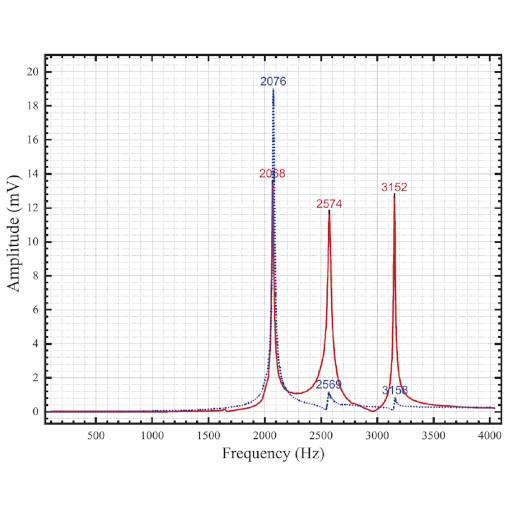
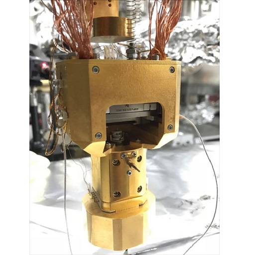
Resonance Frequency of an ANSxy50 made of titanium
attocube scanners, especially the ones made for cryogenic and magnetic environments are often implemented in highly sensitive scanning probe microscopes. One of the major issues in such setups is stability and vibrational stiffness. For such an application, the group of Bert Voigtländer from the institute of Quantum Nanoscience at Forschungszentrum Jülich (Jülich, Germany) detected the resonance frequencies of a standard ANSxy50 positioner made of titanium. The top plate of the scanner was removed for their purpose and the device was fixed on a support. The scanner body was excited with an external piezoelectric element while the response voltage (due to the piezoelectric effect) of the integrated piezo elements detected the resulting vibrations of the scanner. The measurements showed clear resonance peaks at frequencies in the kHz regime, namely 2.1 kHz (1st mode), 2.6 kHz (2nd mode) and 3.2 kHz (3rd mode), showing the high stability of this attocube scanner. Comparing the results with simulations of the resonances idetified these with complex modes with dominant vibrating directions in z (1st mode), and in perpendicular modes in the x-y plane (2nd and 3rd mode). After this successful evaluation, the Jülich group will use these scanners, which combine high stiffness with a large scan range, in a low temperature four-tip scanning probe microscope.
This measurement was realized with the ANSxy50/LT xy-Scanner made from Titanium.
Near-Field Scanning Microwave Microscope at 30mK
Scanning techniques such as atomic force microscopy (AFM) or scanning tunnelling microscopy (STM) offer a wide range of material investigation possibilities. Depending on the environmental conditions and the required scanning resolution scanning probe microscopes are hard to design and setup and not seldom homemade devices, adapted to their special proposes and requirements. A new low temperature near-field scanning microwave microscope working at 30 mK, designed to meet emerging needs of the quantum technologies sector, was now developed by the group of Sebastian de Graaf at NPL (National Physical Laboratory, Teddington, UK) in collaboration with the group of Prof. Sergey Kubatkin (Chalmers University of Technology, SE). It combines microwave characterization up to 6 GHz with STM or AFM techniques. The environment of a dilution cryostat makes special demands on the stability and stiffness of the used components. The group used a set of ANPx100 and ANPz100 nanopositioners (former versions of the ANP101 positioners) to align the sample with the tip in x, y, and z direction and a small ANPz51 positioner for the RF waveguide positioning. First verifications of the instrument showed the capability to image dielectric contrast down to the single microwave photon regime.
This measurement was realized with the ANPx101/LT/HV - linear x-nanopositioner, the ANPz101/LT/HV - linear z-nanopositioner, and the ANPz51/LT/HV - linear z-nanopositioner.
Further reading:
S. Geaney et al; Scientific Report 9, 12539 (2019)
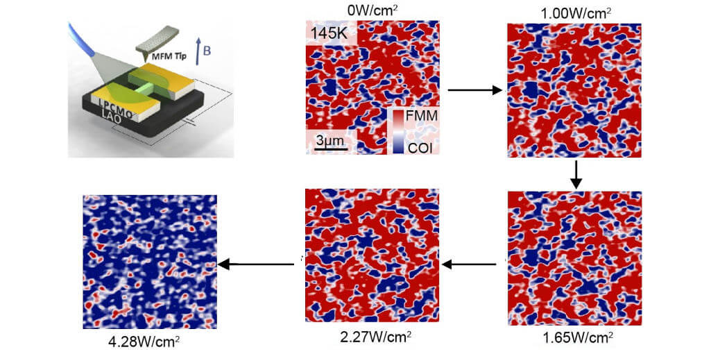
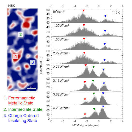
Discovery of Intermediate State in the Metal-Insulator Transition
A closer look at the state configuration of a first-order metal-insulator transition illuminates the coexistence of the metallic and insulating phases at ultra fast timescales. Based on their former work [1] the group of Jian Shen at the Fudan University (Shanghai, CN) witnessed a third long-living intermediate state emerging at the photoinduced first-order metal-insulator transition of La0.325Pr0.3Ca0.375MnO3, building a bridge between the other two states [2].
The attoAFM used in dual pass mode delivered not only the topography of the sample but also the magnetic distribution on the nm scale. Combined with Magneto Optical Kerr Effect (MOKE) measurements the authors identified the third state as a mixture of the ferromagnetic metallic and the charged-ordered insulating states. These findings open the door to create two completely different characteristic length of phase separation in first order metal-insulator transitions. In a next step it will be interesting to see if the results can be adapted to other first-order metal-insulator transitions in different condensed matter systems.
This measurement was realized with the attoAFM I.
Ultimate Thermal Stability and Ultra-Low Drift
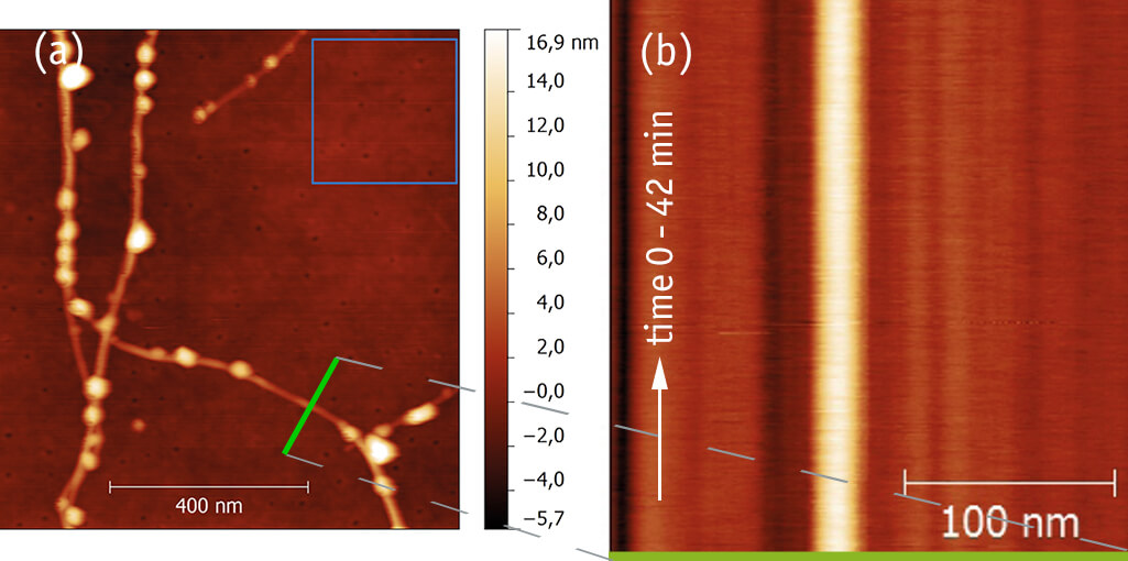
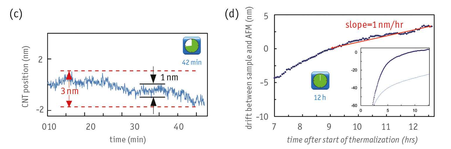
In order to characterize both the low-frequency drift of the atomic force miroscope unit of the attoCSFM with respect to the sample, a carbon nanotube (CNT) was imaged (a). By scanning the same line across the CNT (green line in overview image) 500 subsequent times within 42 minutes (b), a line-to-line position jitter below 1 nm and a long-term drift of less than 3 nm were observed (c), demonstrating the outstanding thermal and mechanical stability of the attoCSFM. After several hours of thermalization, drifts below 1 nm/h can be achieved (d). The part of drift due to scanner creep is constantly monitored interferometrically and can therefore be corrected.
(attocube application labs, 2012; sample courtesy of A. Hartschuh, LMU Munich, Germany)
This measurement was realized with the Combined Atomic Force & Confocal Microscope.
A new way to modulate exciton-complex emissions of TMDs
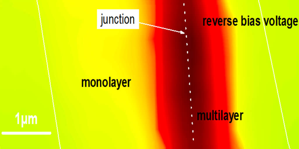
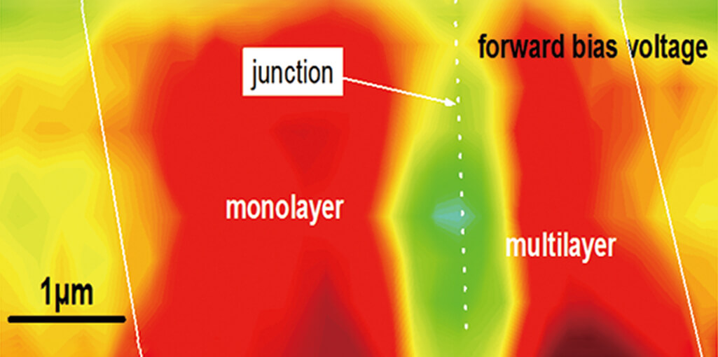
A new type of atomically layered transition-metal dichalcogenides (TMD) was developed by Mr. Taishen Li and co-workers from the University of Science and Technology of China (Hefei, China): a triangular inkslab-like WSe2 homojunction with a monolayer in the inner surrounded by a multilayer frame.Optical and scanning photocurrent microscopy (SPCM) measurements performed with the attoCFM I, cooled by a closed cycle attoDRY1000 to cryogenic temperatures, shows a clear redshift of the photoluminescence peaks from the center to the edge region of the inner monolayer, reflecting a high charge density gradient. In addition, a significant rectifying behavior and photovoltaic response across the homojunction is observed. All in all, the results lead to efficient modulation of the exciton-complex emissions of TMDs.
This measurement was realized with the attoDRY1000, and the attoCFM I.
Further reading:
T. Li, et al., ACS Nano 12 (5), pp 4959–4967 (2018)
Measurements of field-driven transformation of a domain pattern
The group of Erik Folven at the Norwegian University of Science and Technology (Trondheim, Norway) used an attoAFM I for MFM measurements with a closed cycle attoDRY1000 to demonstrate how topological defects may be invoked to understand magnetic domain state transitions. The atomically sharp and magnetized tip of the microscope is scanned across the thin film surface to pick up the out-of plane stray fields from the sample and thus is sensitive primarily to spin textures such as domain walls and defects. The MFM measurements taken at 5K help to understand and describe micromagnetic domain state transitions and to assess their stability in remanence. This insight may open for new approaches to control the switching properties of micro- and nanomagnets.
This measurement was realized with the attoDRY1000, and the attoAFM I.
Further reading:
S. D. Sloetjes, et al., Appl. Phys. Lett. 112, 042401 (2018)
Quantized Conduction on Domain Walls of a Magnetic Topological Insulator
In a paper published in Science, researchers from the University of Tokyo and RIKEN (Japan) have studied “Quantized conduction on domain walls of a magnetic topological insulator” using an attoAFM/MFM in a 3He-cryostat down to 500 mK. In their paper, Yasuda et al. designed and fabricated magnetic domains in the quantum anomalous Hall state, and proved the existence of the chiral one-dimensional edge conduction along the domain walls through transport measurements.
This discovery would permit fully electrical control of the mobile domain walls and chiral edge states, which may lead to the realization of low-power-consumption spintronic, memory and quantum information processing devices in the future.
This measurement was realized with the attoAFM I.
Further reading:
Yasuda et al., Science 358, 1311–1314 (2017)
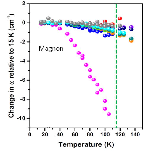
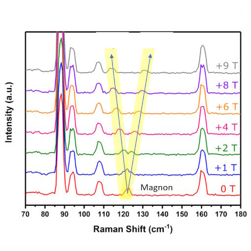
Quasi-2D Magnon identified via Magneto-Raman Spectroscopy
Due to myriad of interesting electronic, mechanical and optical properties, van der Waals materials have been extensively studied in recent years. Exploring their magnetism has been neglected, mainly because of scarcity of long-range magnetic order in 2D materials. Yet, when it exists, like in FePS³, it poses a huge technological potential, particularly since magnetic properties of 2D materials are easily tuneable. The group of Angela Hight Walker at NIST (Gaithersburg, Maryland, USA) developed and used a state-of-the-art cryogenic Raman system cooled by an attoDRY1000 to investigate FePS³ in an antiferromagnetic ordering which leads to a folding of the Brillourin zone and thus to a new modes appearing below the Néel temperature TN. With their temperature and magnetic-field dependent Raman spectra, the group established that one of the appearing modes can only be explained as a magnon and not with a phonon, contrary to previous assumptions. The magnon frequency was detected at 3.7 THz which is an order of magnitude faster than in the previously studied MnPS3. To the best knowledge, this is the first verification of a quasi-2D magnon in a layered material by magneto-Raman spectroscopy.
This measurement was realized with the attoDRY1000, and the attoCFM I.
Further reading:
A. McCreary et al., Phys. Rev. B 101, 064416 (2020)Press release
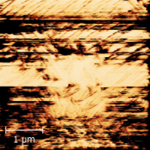
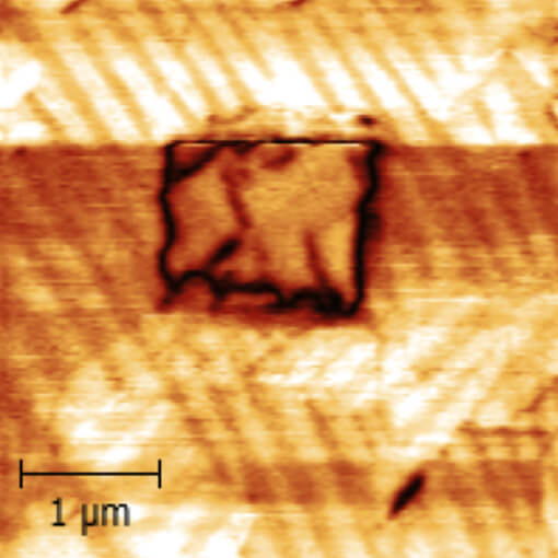
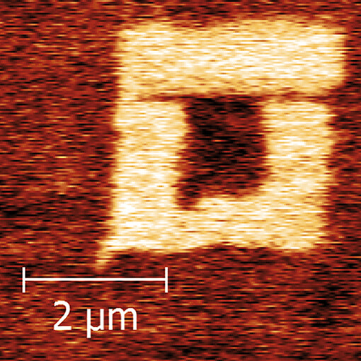
Local Conductivity Mapping and PFM on BFO Thin Film
In this application, the versatility of the cryogenic attoAFM I was demonstrated on an ultra-thin film of BFO. A simple box writing and reading measurements was performed. During the writing phase, a DC voltage of -10 V was applied to write a box. For the reading, a 5 Vpp AC excitation at ≈42 kHz on top of a -2 V DC voltage was used. Combining both AC and DC voltage at the same time allows for a simultaneous measurement of PFM (right image) and local conductivity (left image).
(attocube application labs, 2014; sample courtesy of N. Domingo, ICN Barcelona, Spain)
This measurement was realized with the attoAFM I.
Low Temperature Piezoresponse Force Microscopy on BiFeO
Piezoresponse Force Microscopy (PFM) is a standard tool at room temperature to investigate new materials, especially multiferroics. However, in many cases the scientifically interesting phases only exist at low temperatures or high magnetic fields, what demands the extension of this technique to extreme conditions. In collaboration with our customers, we adapted our attoAFM based on the general purpose ASC500 for PFM measurements. In the measurements shown on the left, we investigated BiFeO3 a well know room temperature multiferroic. The figure shows piezoresponse amplitude after a box in the box writing at 160 K on the sample.
(attocube application labs, 2013; Sample courtesy of Neus Domingo & Gustau Catalan, CIN2 Barcelona, Centre d’Investigació en Nanociència i Nanotecnologia, Bellaterra, Spain)
This measurement was realized with the attoAFM I.
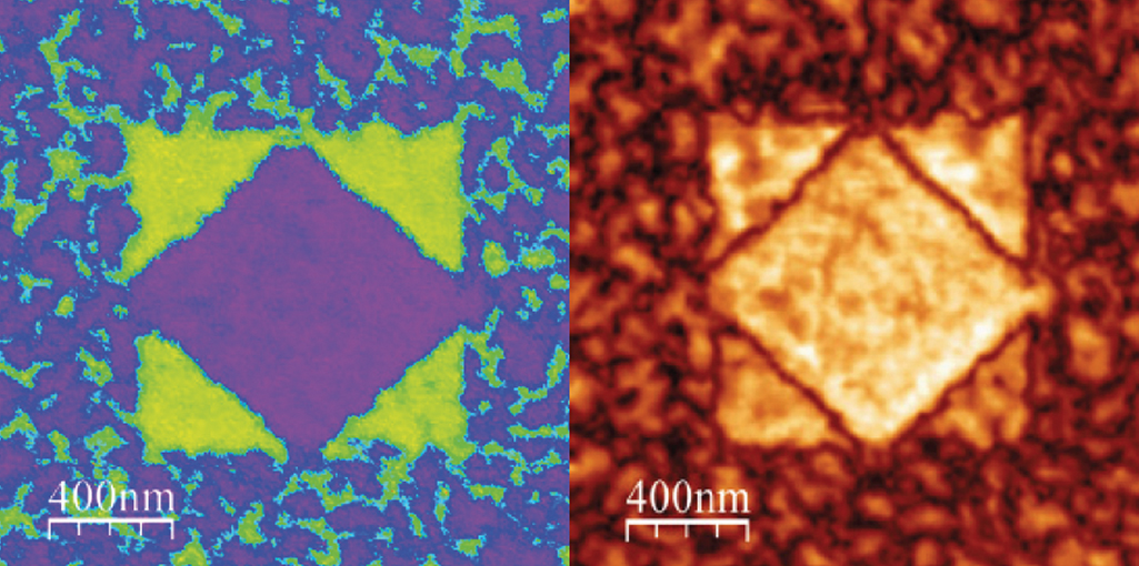
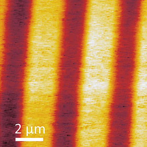
Piezo-Response Force Measurements on Ferroic Oxide Films
The renaissance of multiferroics in which at least two ferroic or antiferroic orders coexist, is motivated by fundamental aspects as well as by their possible applications in the field of spintronics. Magnetoelectric coupling allows for instance the reversal of the ferroelectric polarization by a magnetic field or the control of the magnetic order by an electric field. Most of the ferromagnetic-ferroelectric compounds exhibit both orders at low temperature.
In the measurements presented here PFM data have been taken on a layered heterostructure (150 nm BiFeO3-Mn on top of 35 nm of SrRuO3 on a SrTiO3 (001) substrate) recorded at 82 K with a standard attoAFM I. Two squares have been written, a 1 x 1 µm2 and a smaller, rotated one with ±15 V tip voltage. It can be noted that the amplitude goes to zero in the domain walls and that the outside area shows natural domains.
(Images and data courtesy of K. Bouzehouane and S. Fusil, Unité Mixte de Physique CNRS/Thales, Paris, France)
This measurement was realized with the attoAFM I.
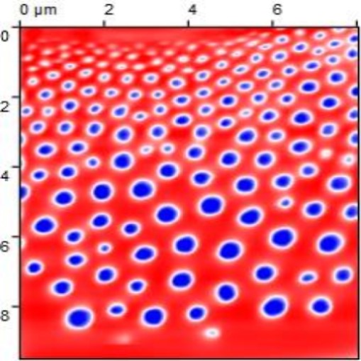
Dynamic Visualization of Nanoscale Vortex Motion using attoSTM in an attoLiquid3000
Matias Timmermans and co-workers invented an innovative technique removing the lack of temporal resolution in STM imaging. They used an attoSTM in an attoLIQUID3000 3He cryostat to measure and study vortex motion in 2H-NbSe2 on a much shorter time scale. By applying a small AC magnetic field they induced a periodic movement of the vortices. The external perturbation results in a distinct smearing of the vortex in the images. Instead of collecting several consecutive images, the tunnelling current is recorded at each point over three cycles of the excitation. The exceptional thermal and spatial stability of the attoSTM in the attoLiquid3000 allows further analysis of the time dependence of this signal at each point. Using an additional lock-in technique more details and understanding of the vortex motion is revealed. By mapping the first and a second harmonic of the tunnelling signal (see upper figures), they were able to visualize changes of the vortex lattice when the vortex density is increased by increasing the DC magnetic field.
In a next step, they used the AC excitation as a time reference to track the motion of individual vortices in time. This results in time resolved snapshots of the vortex motion, which allows them to construct a movie frame by frame. This visualization procedure is unprecedented and promises a much better understanding of the dynamical behaviour of the superconducting condensate (see lower figures). Contrary to the expectation the vortex does not move in a line but follows a circular motion, due to a potential created by atoms and/or vortices.
This measurement was realized with the attoAFM III.
Low Temperature Surface Piezoelectricity in SrTiO3 using Piezo-Response Force Microscopy
SrTiO3 is one of the most investigated materials from the ferroelectric perovskite titanates family due to the variety of physical phenomena ranging from incipient ferroelectricity to superconductivity. Nowadays, considerable interest to SrTiO3 is conditioned by the observations of additional anomalies in the quantum paraelectric regime of SrTiO3, which could be described in terms of a coherent quantum state occurring below T≈37 K. It is supposed that these anomalies are related to the existence of large polarization clusters. Visualizing the dynamic of ferroelectric nanoscale structure at low temperatures may shed light on the mechanisms of the T≈37 K anomaly.
This measurement was realized with the attoAFM I.
Scanning Hall Probe Microscopy at 300 mK with ANP positioners
The magnetic properties of superconducting and ferromagnetic materials at ultra-low temperatures represent some of the most interesting contemporary problems in condensed matter physics. These properties are typically investigated using a magnetic force microscope or a scanning Hall probe microscope (SHPM). In this note, we report on a self-built SHPM capable of working at temperatures as low as 300 mK and magnetic fields of up to 10 T, while still having sub-micron lateral spatial resolution.
This measurement was realized with the ANPx101/LT - linear x-nanopositioner, and the ANPz102/RES/LT - linear z-nanopositioner.
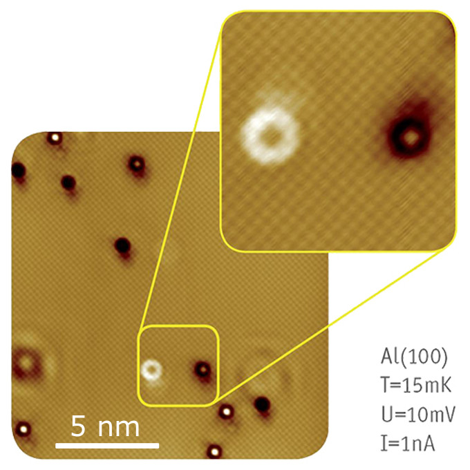
mK STM Image with Atomic Resolution
STM image of an aluminum (100) surface with atomic resolution. The image size is about 29 x 20 nm2. The corrugation is between 300 fm and 800 fm, depending on the direction of the line profile. Defects show up as ring-like structures with different radii depending of their depth. The image was measured in a homebuilt mK-STM at the Max-Planck Institute for Solid State Research in Stuttgart, which uses a cryogenic attocube ANPz51 positioner for coarse approach.
(Image courtesy of Department of K. Kern, Max-Planck Institute for Solid State Research, Stuttgart, Germany)
This measurement was realized with the ANPz51/LT - linear z-nanopositioner.
Piezo-Controlled Exfoliation of Graphene
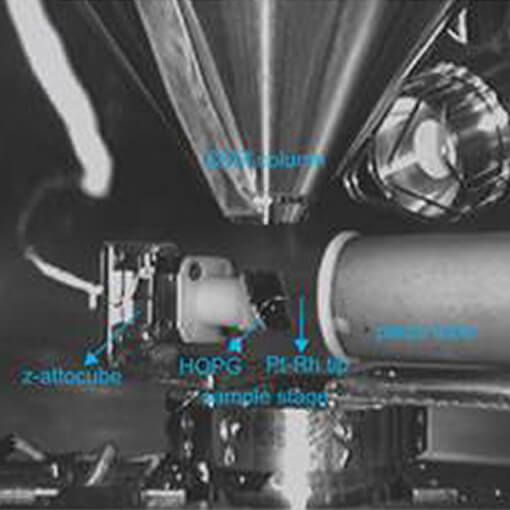
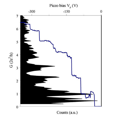
In the group of Prof. Gosh at the IIS in Bangalore, researcher Kinikar and his coworkers managed to measure the conductance of narrow stripes of graphene during their exfoliation. A metal tip is crashed into a graphite HOPG crystal using an attocube positioner for vacuum application, namely the ANPz101, and slowly retracted via a piezo tube. Conductance is measured from the tip through the HOPG crystal. The setup situated inside a SEM is shown in picture 1. The graphite piece sticking on the tip will thereby be torn to a single layer of graphene. Mechanically torn graphene has highly crystalline edges, leading to quantized conductance. This is due to one-dimensional channels forming at the edges each with a conductance of 2e2/h (graph 2). A similar setup was used in a cryostat for high magnetic field measurements.
Kinikar: “The attocubes have been with us for over a decade, and they still work perfectly!”
Further reading:
A Kinikar et al; Nature Nanotechnology 12, 564-568 (2017).
HF-SPM using attocube nano-positioners in magnetic fields above 30 T
In an outstanding setup, Benjamin Bryant and Lisa Rossi (High Field Magnet Laboratory, Radboud University, Nijmegen, NL), together with the SPM group of Alex Khajetoorians (Radboud University), designed a high field scanning probe microscope (HF-SPM) for operation at cryogenic temperatures and in extreme magnetic fields up to 38 T. The high magnetic field is provided using a water-cooled Bitter magnet: noise from the cooling water creates a highly challenging vibration environment for SPM. An ANPz30 nanopositioner controls the coarse approach of an atomic force microscope cantilever to a scanned sample. The attocube positioner provides for a modular design that makes it easy not only to change the components if needed but also allows the flexibility to employ different cantilever or sample holders. Due to the compactness and rigid design of the positioner the sensitivity to vibrational noise is reduced, which is critical for SPM in the extreme environment of the Bitter magnet.
This measurement was realized with the ANPz30/LT - linear z-nanopositioner.
Conductive-Tip AFM Measurements on Ruthenium
In this application, atomic steps on Ruthenium were investigated using conductive-tip AFM. Atomic steps as well as spiral dislocations can be identified on the molecular beam epitaxy-grown sample. The contrast in this measurement is highly enhanced due to a difference in conductance between edges and flat plateaus. Such high contrast was not observed in the accompanying topographic image. A voltage of +10 mV was applied to the standard Pt-coated AFM tip, while the sample was grounded via a current amplifier with gain 106 V/A. The measurement was performed at room temperature in a 20 mbar He atmosphere.
(Sample and measurement courtesy of V. Da Costa, J.-F. Dayen, B. Doudin, IPCMS-DMONS,CNRS/University of Strasbourg, France)
This measurement was realized with the attoAFM I.
KPFM of Au-on-Pt Pattern
The kelvin probe force microscopy (KPFM) measurements shown here were performed on a test sample consisting of a Au layer on a Pt substrate in dual pass mode at cryogenic temperatures of 4K. The KPFM image was recorded during the second line with a lift height of about 50 nm. The color scale spans approximately 130 mV, and the image size is 11.9 µm x 11.9 µm.We found a KPFM contrast of approx. 35 mV, and a KPFM resolution (noise level) of approx. 2.6 mV.
(attocube application labs 2014)
This measurement was realized with the attoAFM I.
attoAFM/CFM in Toploading Insert
The presented data was taken with a mk-compatible version of the attoAFM/CFM mounted on a toploading insert of a Leiden Cryogenics closed-cycle dilution refrigerator. The sample temperature was 60 mK during an AFM scan with a speed of 400nm/s. The images nicely demonstrates that the delicate microscope works very well even under these extreme conditions.
This measurement was realized with the attoAFM/CFM.
Tuning Fork based AFM measurements at cryogenic temperatures
The attoAFM III is a tuning fork based setup for highly precise low temperature measurements. The non-optical design faciliates e.g. measurements on light-sensitive samples using conductive STM-type tips.
The distance feedback is done by detecting the tuning fork vibration using a Phase-Locked Loop (PLL) together with a feedback loop. The PLL tracks the resonance of the tuning fork, whereas the feedback loop keeps the z-distance in such way that the frequency shift (vs. the free oscillation) remains at a certain level.
The presented data was measured using uncapped, stacked InAs Quantum Dots in a GaAs matrix with an attoAFM III inside an attoLIQUID.
This measurement was realized with the attoAFM III.
Scanning Tunneling Spectroscopy and Vortex Imaging on NbSe2 with attoAFM III / STM I at 315 mK
Scanning Tunneling Spectroscopy (STS) is a useful tool to characterize material properties, especially on superconductors at ultra low temperatures. In a series of experiments STS measurements as well as vortex imaging on NbSe2 have been performed at a temperature of only 315 mK. The tests show excellent stability of the combined attoAFM/STM microscope setup as well as the possibility to apply stable voltages in the micro-Volt range.
This measurement was realized with the Tuning-fork-based AFM for Scanning Gate Microscopy.