

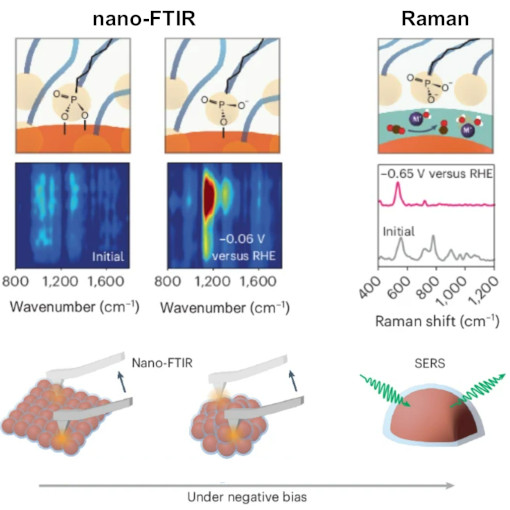
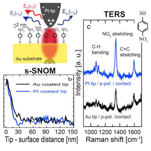
Interface nano-Electrochemistry Study
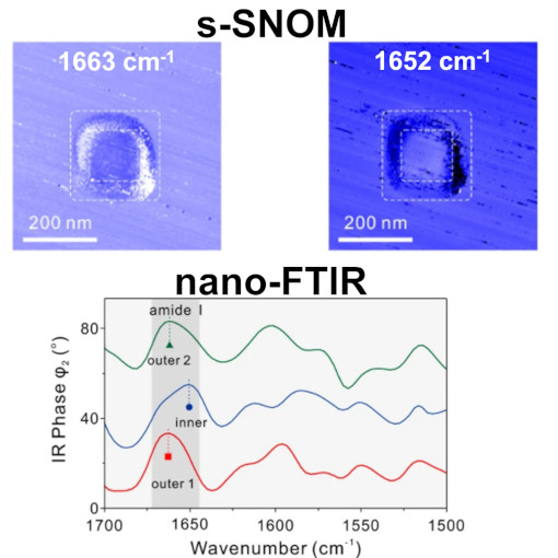
Recent advancements in nanocatalysis have been significantly bolstered by the application of nano-FTIR (infrared nanospectroscopy) and surface-enhanced Raman spectroscopy (SERS), providing unprecedented insights at the molecular level. nano-FTIR, especially valuable due to its high spatial resolution, has elucidated the electrochemically driven transformation of ligands on nanoparticles, which is crucial for creating active microenvironments for reactions like CO2 to CO conversion. This transformation involves the detachment and reconfiguration of ligands, a process dynamically captured through the concurrent use of nano-FTIR and SERS. The integration of these techniques allows for a detailed observation of ligand dynamics and the formation of an electrocatalytic interlayer, highlighting the importance of precise molecular arrangement for enhancing catalytic efficiency.
nano-FTIR, when combined with Raman spectroscopy, underscores the pivotal role of controlled ligand behavior in steering the selectivity and activity of nanocatalytic processes.
This measurement was realized with the IR-neaSCOPE+TERs.
Further reading:
Yu et al., Nature Catalysis 2380, 9 (2024)
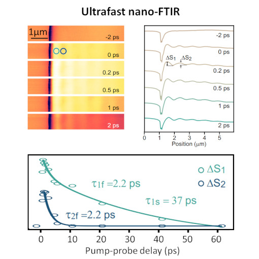
Plasmons Revolutionize Optoelectronics
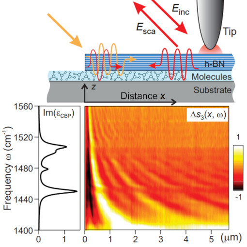
In recent developments, researchers from multiple prestigious institutions across China have significantly advanced optoelectronics by harnessing the properties of hyperbolic transient plasmons in black phosphorus (BP), a material known for its unique anisotropic electronic and optical characteristics. This advancement comes from the ability to manipulate BP's charge carriers, enabling hyperbolic plasmon polaritons and overcoming previous challenges associated with hyperbolic polariton materials. The breakthrough involved a topological transition in BP's dielectric tensors through photo-induced carrier injection, making it possible to transform its iso-frequency contour and unlock the potential of rare transient hyperbolic plasmons. These plasmons exhibit ultrafast transitions, minimal propagation losses, and efficient optical emissions.The ultrafast nano-FTIR nanoscopy technique has been pivotal in revealing transient plasmonic phenomena at the nanoscale, driving innovations in optoelectronics, photonic circuits, sensors, and energy systems through the dynamic modulation of BP's properties.
This measurement was realized with the IR-neaSCOPE+fs.
Further reading:
Fu et al., Nature Communications 15, 709 (2024)
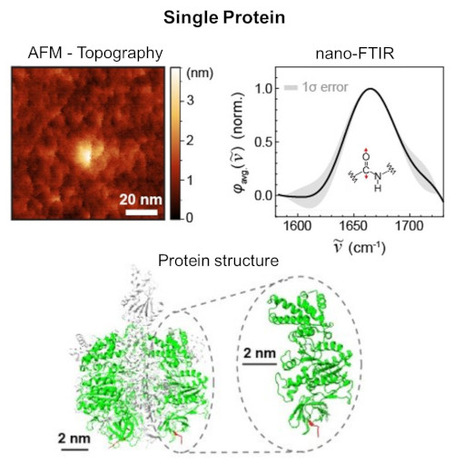
Single Protein IR Nanospectroscopy
The article from the Institute for Molecular Science discusses a breakthrough in observing single proteins using nano-FTIR, enabling the detection of infrared vibrational spectra of a single protein. This advancement allows for analyzing extremely small samples, which was previously challenging with conventional methods. The research is significant for understanding protein functions and interactions, and it opens new possibilities in nanoscale infrared spectroscopy applications across various fields. The study represents a major step in ultra-sensitive and high-resolution imaging using mid-infrared light.nano-FTIR, as demonstrated in the study, opens up diverse applications in fields like molecular biology for precise protein analysis, materials science for nanomaterial characterization, and medical diagnostics for identifying molecular markers in diseases.
This measurement was realized with the IR-neaSCOPE+s.
Further reading:
Nishida et al., Nano Lett. 2024
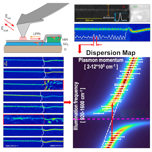
Unveiling Polariton Pulse Dynamics
This study explores polariton pulses - unique light-matter waves - and their complex behaviors in anisotropic media, driven by ultrafast and minuscule field changes. Using innovative time-resolved nanoimaging and advanced data processing, researchers have unveiled fascinating spatiotemporal dynamics, like curved energy flows and differing wave and energy velocities.The paper highlights the inadequacies of current technologies in capturing these rapid, directional, and nanoscale phenomena. The breakthrough nano-FTIR technology overcomes these limitations, enabling detailed visualization and analysis of polariton pulse behaviors. This advancement paves the way for transformative developments in ultrafast nanoimaging, with implications for molecular sensing, hyperlensing, and nanophotonic energy control.In summary, this research opens new horizons in optics and material science, from investigating intricate space-time dynamics at unprecedented scales to advancing ultrafast nanoimaging, marking a significant leap in the field.
This measurement was realized with the IR-neaSCOPE+fs.
Further reading:
Zhang et al., Science Advances 9, eadi4407 (2023)
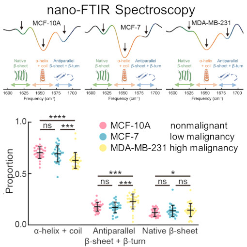
nano-Vesicle Tumor Diagnostic
Cells communicate by releasing tiny, membrane-bound vesicles, pivotal in transmitting bioactive molecules. These vesicles are not just cellular messengers; they play a crucial role in the development and spread of tumors. One intriguing aspect of these vesicles is their protein composition, which changes in correlation with the severity of malignancy. This study dives into this world of microscopic communication using nano-FTIR to examine the subtle differences in individual small extracellular vesicles related to cancer.Xue et al. discovered that as a tumor becomes more malignant, the ratio of amide I/II absorption in these vesicles increases. Ratio which corelates directly with the decrease in a-helix and random coil structures and increase of ß-sheet and ß-turn structures. The use of nano-FTIR spectroscopy is proving to be invaluable in detecting these small but critical variations. This research paves the way for a novel, noninvasive approach to understanding cancer's progression. It holds the promise of uncovering new biomarkers for cancer, potentially revolutionizing early detection methods.
This measurement was realized with the IR-neaSCOPE+s.
Further reading:
Xue et al., J. Am. Chem. 144, 20278 (2022)
cryo-Tuning Surface Phonon-Polaritons
This research explores how adjusting the temperature and electrical properties affects surface phonon-polaritons in LaAlO3/SrTiO3 heterostructures, a promising area in nanophotonics. A significant contribution to this study is the use of nano-FTIR and s-SNOM techniques. Nano-FTIR allowed for detailed spectroscopic analysis at the nanoscale, enhancing the understanding of surface phonon-polaritons in these materials. The s-SNOM technique was pivotal in imaging and probing the properties of phonon-polaritons, providing crucial insights into their behavior under varying thermal and electrostatic conditions. This research underscores the potential of LaAlO3/SrTiO3 heterostructures in nanophotonic applications, bridging the gap between unconventional electronics and long-wavelength nanophotonics. The findings demonstrate the tunability of phonon-polariton properties, paving the way for advancements in infrared technology and material science.
This measurement was realized with the cryo-neaSCOPE+xs.
Further reading:
Zhou et al., Nature Communications 14, 7686 (2023)
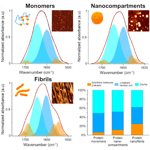
Nano-to-Micro Silk Fiber Morphing
Silk is a uniquely strong biomaterial, remarkable for its simple protein components. Despite numerous attempts, replicating silk synthetically remains a challenge. A groundbreaking discovery in silk fiber production was the formation of nanoscale compartments. These compartments facilitate a reversible transformation of silk proteins. They transition from their native structure into crystalline ß-sheets, a process that can be reversed. This reversibility is key to modifying the final mechanical properties of silk, opening doors to custom-tailored silk products. This customization is achieved by controlling the silk proteins' structural changes and their self-assembly into larger molecular formations.nano-FTIR spectroscopy has enabled researchers to closely examine protein structures at the nanometer level. This technique is especially beneficial for analyzing protein complexes and the stages of protein aggregation into fibers. It combines the morphological insights from AFM with the detailed structural information from FTIR spectroscopy. The team conducted qualitative tests with nano-FTIR spectra on different protein structures - from individual monomers to nanocompartments and fibrils - confirming the effectiveness of their method.This synergy of nano-FTIR spectroscopy and atomic force microscopy has been pivotal in deciphering the reversible transitions of silk proteins. It's a cornerstone in the journey towards developing more sophisticated and versatile silk-based materials.
This measurement was realized with the IR-neaSCOPE+s.
Further reading:
Eliaz et al., Nature Communications 13, 7856 (2022)
Polaritons Defy Symmetry
Nanoscale polaritons are crucial for nanophotonic devices. Hyperbolic polaritons (HPs) in high-symmetry crystals often lack directionality. In a recent eLight publication, scientists led by Profs. Zhang, Li, and Dai introduced a technique for anisotropic HP excitation and propagation. They discovered hyperbolic shear polaritons in low-symmetry crystals with enhanced directional propagation. This approach allows control of HPs' mirror symmetry without needing low crystalline symmetry. It enables tunable asymmetric polariton propagation, expanding possibilities for nanoscale light control and reconfigurable polaritonic devices.Introduced method breaks mirror symmetry in crystal polaritons, enabling control of asymmetry in HP responses. Offers nanoscale light manipulation and potential applications in nanoimaging, photonics, and quantum physics.
This measurement was realized with the IR-neaSCOPE+s.
Further reading:
Hu et al, eLight 3, 14 (2023)
SciTechDaily Article
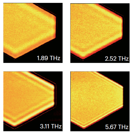
THz Plasmon Polaritons
Plasmon polaritons are quasiparticles resulting from the coupling of surface plasmons with light. Such Polaritons possess tremendous potential for investigating essential material properties and advancing the field of nanophotonics by enabling the creation of innovative devices. However, the direct observation of ultraconfined in-plane anisotropic plasmon polaritons has proven to be a scientific and technological challenge until now. With this publication, the authors used s-SNOM to image ultraconfined in-plane anisotropic THz plasmon polaritons in a narrow-bandgap semiconductor with strong anisotropy. By placing the platelets above a gold layer, the hybridization of plasmon polaritons with their mirror image enhances the direction-dependent propagation length and confinement of the polaritons. The THz s-SNOM images of the Ag2Te/SiO2/Au heterostructure reveal up to three narrow polariton fringes parallel to the edges. These findings expand the control and manipulation of polaritons, offering potential for nanoscale photonic devices and applications.
The study demonstrates the use of THz plasmon polaritons for measuring anisotropic charge carrier masses and damping.
This measurement was realized with the THz-neaSCOPE+s.
Further reading:
Chen et al., Nature Materials 84, 2869 (2023)
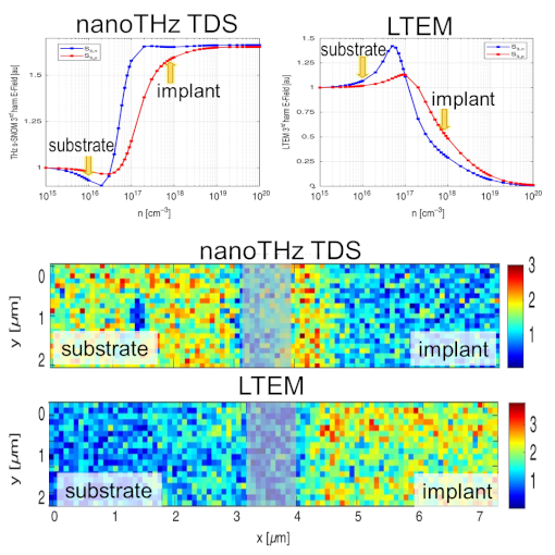
Laser THz Emission Microscopy
s-SNOM has revolutionized subwavelength optics by coupling electromagnetic radiation to a sharp subwavelength metal tip, held near a surface, and measuring the scattered radiation. This technique has had a significant impact in the infrared and terahertz regions of the spectrum. However, coupling short-wavelength radiation to the nanoscale tip has been challenging, hindering the study of wide-bandgap materials such as Si and GaN. In this study, the first s-SNOM measurement exceeding 3?eV photon energy was achieved, allowing the use of tightly focused blue light for nanoscale resolution. This technique, known as laser terahertz emission microscopy (LTEM), offers exciting new possibilities for the application of s-SNOM methods to wide-bandgap materials.In summary LTEM spectroscopy and imaging, providing an avenue to directly observe charge carrier properties in materials not amenable to THz s-SNOM techniques.
This measurement was realized with the THz-neaSCOPE+s.
Further reading:
Pizzuto et al., Light: Science and Applications 12, 96 (2023)
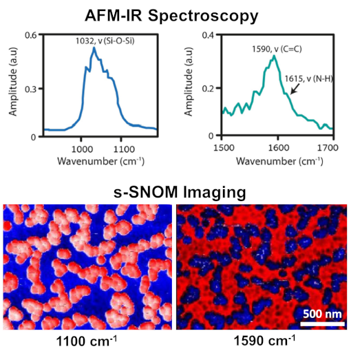
Nanoparticle Imprinted Matrices
Nanoparticle-imprinted matrix is an innovative approach that allows for the selective detection of nanoparticles based on their size, shape, surface chemistry, and composition. However, those systems have mainly been used for detecting metallic nanoparticles such as Au or Ag by electrochemical dissolution. This study applies s-SNOM imaging and AFM-IR spectroscopy to characterize the physical entrapment of silica-NPs by the matrix at the nanoscale. Point IR spectra collected from a 20 nm radius identified the vibrations of the aromatic C=C bond and the amine group of the poly(3-aminophenol) matrix, as well as the Si-O-Si vibration of the silica nanoparticles. In addition, IR-sSNOM imaging at specific wavenumbers demonstrated the intricate dispersion of silica-NPs enclosed by the matrix and revealed the chemical and vibrational contrast in the nanoscale between the organic matrix and the inorganic nanoparticles.In summary, the use of AFM-IR and s-SNOM technologies in this study provided unique insights into the electrochemical reduction of CO2 to CO and demonstrated the power of these advanced analytical techniques for the investigation of complex chemical reactions.
This measurement was realized with the IR-neaSCOPE.
Further reading:
Dery et al., ChemElectroChem e202300039, (2023)
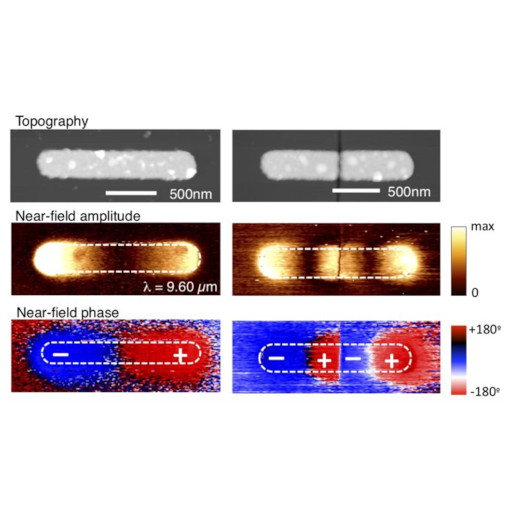
Analyzing Optical nano-Antennas
Near-field microscopy can be used to analyze the local field of photonic structures. Near-field images of a resonant (verified by far-field spectroscopy) antenna exhibit the clear signature of a dipolar oscillation mode on the Au rod. Note that the probing tip preferentially selects the z-component (normal to the sample surface) of the optical field. The amplitude image exhibits a high signal at the rod ends which are 180° out of phase. If the antenna structure is modified by e.g. a cut at the centre of the Au rod (fabricated by FIB), the near-field images reveal two dipolar oscillation modes on the segments. Systematic studies allow to analyze the coupling between the segments and to characterize the optical properties of the antenna structures. Polarized measurements allow to filter out specific components of the optical field associated to photonic structures or devices and to investigate the field e.g. in the antenna gap.
This measurement was realized with the VIS-neaSCOPE+s.
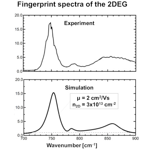
Fingerprint Cryogenic Nanoscopy
2D electron gases (2DEG) are promising confined electron systems for nanoelectronics and quantum technology. However, their sensitivity to defects can result in nanoscale inhomogeneities, posing a significant challenge. To address this issue, the authors utilized cryogenic nanoscopy with s-SNOM point spectroscopy at 8 K to record 2DEG fingerprint spectra in the previously inaccessible spectral window of 700 – 900 cm-1. Within this spectral region, three characteristic peaks were identified, each differently influenced by 2DEG carrier concentration and mobility. This allows for their disentanglement from spectroscopic measurements, providing a deeper understanding of the system's behavior. Notably, rising 2DEG mobility primarily affects the main fingerprint peak around 750 cm-1, with a saturation of the influence around µ = 80 cm2/Vs.
Overall, the presented cryogenic nanoscopy technique based on s-SNOM fingerprint method holds promise as a useful tool for studying confined correlated electron systems in nanoelectronics and quantum technology. Its applicability to other systems suggests broad potential impact in the field.
This measurement was realized with the cryo-neaSCOPE+xs.
Further reading:
Barnett et al. arxiv full text
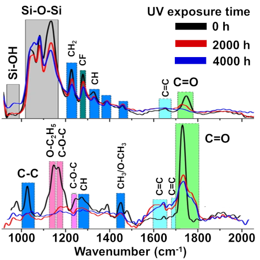
Coating Protects Ancient Pottery
Neolithic Cucuteni ceramic pottery is a valuable artifact that requires proper protection to ensure its preservation for future generations. In this study, polymer nanostructured material is used as protective coatings for the conservation of such ancient artefacts against UV ageing. In the context of comparative evaluation of the protective efficiency, this article reports the use of a functional coating that operates via specific photochemical transformations at the coating-air interface as a UV resistant protection coating for cultural heritage artefacts. An important finding was related to the decrease of the carbonyl band from 1739 cm-1 and to the appearance of other two additional bands located at 1718 (saturated aliphatic ketone) and 1712 cm-1 (carboxylic acid dimer). In addition, the loss of ester groups may be considered the main degradation process, as illustrated by the decrease of the intensity and area of the 1739 cm-1 main carbonyl stretching band.
This study reports the first investigation of the photodegradation behaviour of protective coatings through nano-FTIR technique.
This measurement was realized with the IR-neaSCOPE+s.
Further reading:
Oancea et al., Materials Degradation 7, 21 (2023)
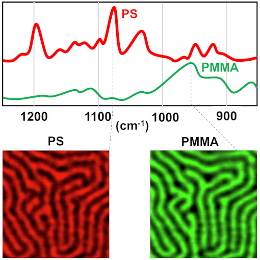
Lamella-forming PS-b-PMMA Films
A non-invasive, image-based analytic method utilizing s-SNOM is suggested to evaluate the phase separation behavior of lamella-forming PS-b-PMMA block copolymer films. Taking advantage of the penetrability of the tip-enhanced IR signal into the films, the spatio-spectral maps of each component are constructed. Subsequently, the effect of a sole and combinatorial applications of the self-assembly procedures, such as solvent vapour annealing (SVA) and/or thermal annealing (TA), on the spatial distribution of PS or PMMA components is quantitatively assessed in terms of the areal portions of the PS domain, PMMA domain, and the mixed zone that is adjacent to the domain border. Additionally, by statistically comparing the local concentration profiles, the chemical contrast between the domains turns out to be dependent upon the annealing procedures (namely, SVA and SVA+TA).
s-SNOM technique can pave the way to an uncomplicated but precise investigation of the polymer nanostructure-based thin film devices, whose performances are critically governed by the spatial arrangement of the chemical elements.
This measurement was realized with the IR-neaSCOPE.
Further reading: Kim et al., Spectrochimica Acta Part A 274, 121095 (2022)
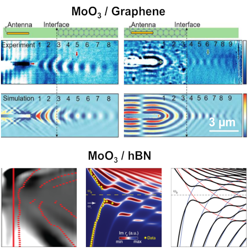
Nanoscale Negative Refraction
Refraction is a familiar effect in which a light beam alters direction as it propagates from one medium to another. Negative refraction is a nonintuitive but well-established effect in which the light beam is bent in the “wrong” direction. Two groups now independently demonstrate negative refraction at the interface of two-dimensional van der Waal materials. Hu et al. used molybdenum trioxide with a graphene MoO3 / Graphene overlayer to show that in-plane negative refraction of mid-infrared (mid-IR) polaritons occurs at the interface and is gate tunable. Sternbach et al. used molybdenum trioxide/hexagonal boron nitride MoO3 / hBN bicrystals to show that negative refraction of mid-IR polaritons occurs for propagation normal to the interface.
Polaritonic negative refraction in the mid-IR provides opportunities for optical and thermal applications such as IR super-resolution imaging, nanoscale thermal manipulation, and chemical sensing devices with enhanced sensitivity.
This measurement was realized with the IR-neaSCOPE+s.
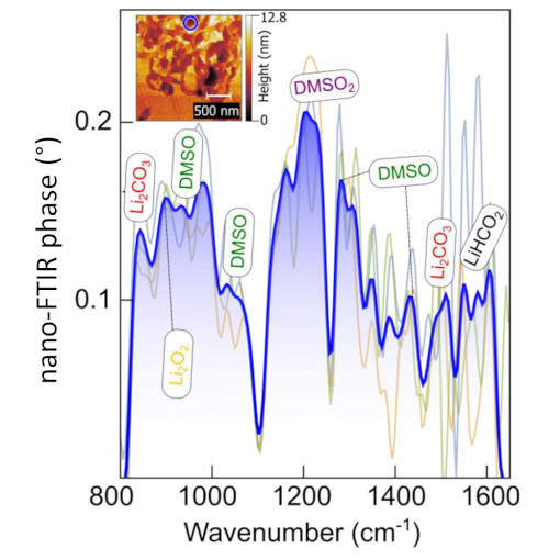
Non-Aqueous Lithium–Air Cells
Metal–air batteries, such as Li–air, may be the key for large-scale energy storage as they have the highest energy density among all electrochemical devices. However, these devices suffer from irreversible side reactions leading to battery failure, especially when ambient air is used as the O2 source. This study uses nano-FTIR to track the chemical composition changes at the nanoscale of electrode surface during cell discharge. The results obtained here open an instructive operando chemical analysis of the Li–Air battery development. The authors observed a high sensitivity to humidity and CO2 in atmospheric conditions, and that the interaction between DMSO and carbon nanotubes (CNT) generates formate species. From 140 s of operation, the DMSO presented a low decomposition rate that remained the same until the end of the discharge.
nano-FTIR is an important tool to study complex discharge processes typically found in conversion batteries, as the case studied here for Lithium–Air.
This measurement was realized with the IR-neaSCOPE+s.
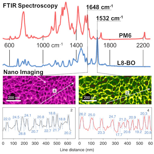
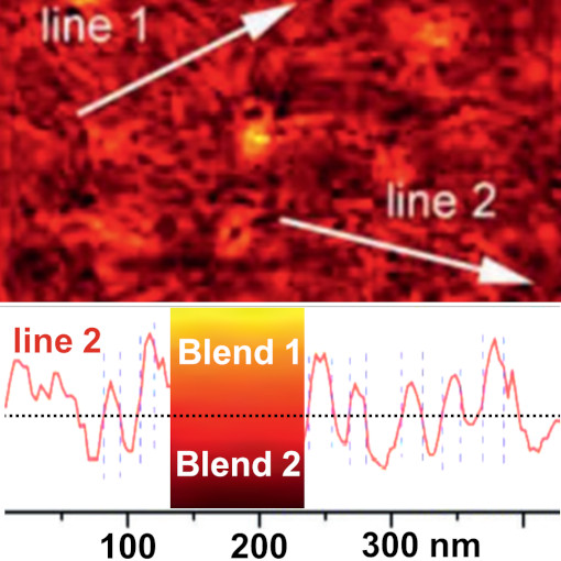
High-efficient Organic Photovoltaics
In organic photovoltaics, morphological control of donor and acceptor domains on the nanoscale is the key for enabling efficient exciton diffusion and dissociation, carrier transport and suppression of recombination losses. This publication demonstrates a double-fibril network based on a ternary donor–acceptor morphology with multi-length scales constructed by combining ancillary conjugated polymer crystallizers and a non-fullerene acceptor filament assembly. Essential for this study was the nanoscale infrared image of double-fibril network PM6/L8-BO with strong IR contrast at 1648/1532 cm-1. In addition, the line profiles across the image was used to estimate a fibril diameter of 22.1 and 22.6 nm for acceptor and donor fibrils concluding that the volume of the mixing domain is low, resulting in low geminate recombination and a high fill factor.
To summarize, double-fibril network morphology strategy minimizes losses and maximizes the power output, offering the possibility of 20% power conversion efficiencies in single-junction organic photovoltaics.
This measurement was realized with the IR-neaSCOPE.
Further reading:
Zhu et al., nature materials 21, 656 (2022)
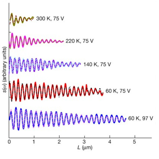
Cryogenic boost to graphene plasmonics
Scientists use graphene plasmon polaritons to squeeze the energy of long-wavelength radiation at the nanoscale and access several quantum effects with wide application range from fundamental research to industry (e.g. lasing, topological protection or dipole-forbidden absorption). The common tool for investigating and optimizing such processes is s-SNOM, however room temperature studies on this sample-system show strong plasmonic dissipation and prevents us to achieve highly confined modes of long plasmonic lifetimes. This study uses s-SNOM at cryogenic temperatures to bypass those shortcomings and to unravel the fundamental limits of propagating plasmon polaritons in high-mobility encapsulated graphene. Already at 60 °K, the propagation length can exceed 50 plasmonic wavelengths, thus setting a record for highly confined and tunable polariton modes. In this regime, the propagation of plasmon polaritons is primarily restricted by the dielectric losses of the encapsulated layers, with a minor contribution from electron–phonon interactions.
Cryogenic s-SNOM controls the losses in heterostructure engineering applications.
This measurement was realized with the cryo-neaSCOPE+xs.
Further reading:
Ni et al., Nature 557, 530-533 (2018)
Molecular Identity of Catalytic Agent
Unambiguous identification of catalytic poisoning species requires experimental methods simultaneously delivering accurate information regarding adsorption sites and adsorption geometries of adsorbates with nanometer-scale spatial resolution, as well as their detailed chemical structure and surface functional groups. However, to date, it has not been possible to study catalytic sulfur poisoning of metal/metal-oxide interfaces at the nanometer scale without sacrificing chemical identity. In this study, nano-FTIR & s-SNOM identify the chemical nature, adsorption sites, and adsorption geometries of sulfur-based catalytic poisons on a Pd(nanodisk)/Al2O3 (thin-film) planar model catalyst surface at the nanometer scale. In addition, this study reveals striking variations between sulfate species from one nanoparticle to another and even vast alterations of sulfur poisoning on a single Pd nanoparticle.
s-SNOM & nano-FTIR provide critical molecular-level insights crucial for the development of high-performance heterogeneous catalysts with extended lifetimes.
This measurement was realized with the IR-neaSCOPE+s.
Further reading:
Say et al., JACS April 29 (2022)
Luttinger-liquid Plasmons
1D Luttinger-liquid plasmons formed inside carbon nanotubes (CNTs) are long-lived excitations with extreme electromagnetic field confinement. In the past, s-SNOM amplitude studies were limited to semiconducting CNTs which require additional doping. This s-SNOM phase study, allows investigation of metallic carbon nanotubes as they support strong tip-launched Luttinger-liquid plasmons at ambient conditions. The Authors extracted the dispersion relation of the hybrid Luttinger-liquid plasmon–phonon polaritons. The dispersion shows pronounced mode splitting, and an ultrastrong coupling regime with phonons of both investigated substrates, i.e., native silica and hBN. Such strong coupling of quasiparticles allows now applications like induced transparency, polariton lasing, changing of the rate of chemical reactions, or enhanced sensitivity in infrared and Raman spectroscopy
s-SNOM studies of Luttinger-liquid plasmons is an essential application to develop novel low-loss plasmonic circuits for the sub-wavelength manipulation of light.
This measurement was realized with the IR-neaSCOPE+s.
Further reading:
Németh et al., Nano Lett. 22, 3495 (2022)
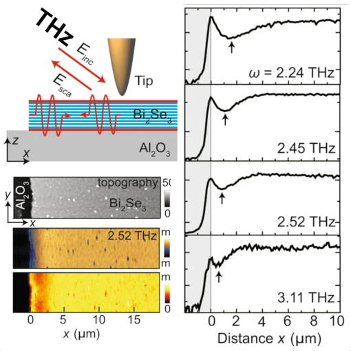
THz Polaritons Nanoimaging
Plasmon polaritons in metals, doped semiconductors and 2D materials have wide application potential for field-enhanced spectroscopies, sensing, imaging, and photodetection. Although polaritons have been observed by many IR s-SNOM studies, real-space imaging of propagating THz polaritons has been missing so far. This study brings the analytical power of s-SNOM to the THz spectral region. In this study, spectroscopic THz near-field images reveal polaritons with up to 12 times increased momenta as compared to photons of the same energy. From the images the authors determine and analyze the polariton dispersion, showing that the polaritons can be explained by the coupling of THz radiation to various combinations of Dirac and massive surface carriers, massive bulk carriers and optical phonons.
THz s-SNOM provides critical insights into the nature of THz polaritons in topological insulators and establishes instrumentation and methodology for imaging of THz polaritons.
This measurement was realized with the THz-neaSCOPE+s.
Further reading:
Chen et al., Nature Communications 13, 1374 (2022)
Solid-State Battery
Solid-state batteries possess the potential to significantly impact energy storage industries by enabling diverse benefits, such as increased safety and energy density. However, challenges persist with physicochemical properties and processes at electrode/electrolyte interfaces. Thus, there is great need to characterize such interfaces in situ and unveil scientific understanding that catalyzes engineering solutions. In this study, the authors conduct multiscale in situ microscopies (optical, atomic force, and infrared near-field) and nano-FTIR of intact and electrochemically operational graphene/solid polymer electrolyte interfaces. They find nanoscale structural and chemical heterogeneities intrinsic to the solid polymer electrolyte initiate a cascade of additional interfacial nanoscale heterogeneities during Li plating and stripping; including Li-ion conductivity, electrolyte decomposition, and interphase formation.
nano-FTIR applies to buried interfaces and interphases in their native environment and readily adaptable to a number of other electrochemical systems and battery chemistries.
This measurement was realized with the IR-neaSCOPE+s.
Further reading:
He et al., Nature Communications 13, 1398 (2022)
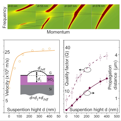
Plasmon in Suspended Graphene
Plasmons in 2D graphene have been invariably studied in supported samples so far. The substrate provides stability for graphene but often causes undesired interactions (such as dielectric losses, phonon hybridization, and impurity scattering) that compromise the quality and limit the intrinsic flexibility of graphene plasmons. This s-SNOM study demonstrate the visualization of plasmons in suspended graphene and introduces the graphene suspension height as an effective plasmonic tuning knob that enables in situ change of the dielectric environment and substantially modulates the plasmon wavelength, propagation length, and group velocity. Such active control of micrometer plasmon propagation facilitates near-unity-order modulation of nanoscale energy flow that serves as a plasmonic switch with an on-off ratio above 14.
The suspended graphene plasmons possess long propagation length, high tunability, and controllable energy transmission simultaneously, opening up broad horizons for application in nano-photonic devices.
This measurement was realized with the IR-neaSCOPE+s.
Further reading:
Hu et al., Nature Communications 13, 1465 (2022)
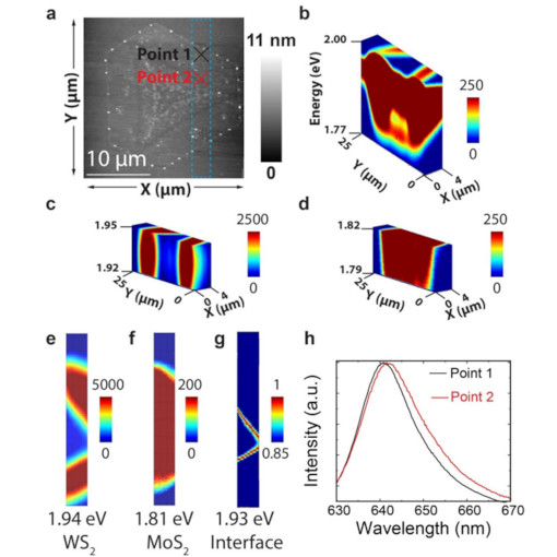
Nano-Interface 2D Alloys
Single-layer heterostructures exhibit striking quasiparticle properties and many-body interaction effects that hold promise for a range of applications. However, their properties can be altered by intrinsic and extrinsic defects, thus diminishing their applicability. Therefore, it is of paramount importance to identify defects and understand 2D materials’ degradation over time using advanced multimodal imaging techniques. Here we implemented a liquid-phase precursor approach to synthesize 2D in-plane MoS2–WS2 heterostructures exhibiting nanoscale alloyed interfaces and map exotic interface effects during photodegradation using a combination of hyperspectral tip-enhanced photoluminescence and Raman and near-field nanoscopy. Surprisingly, 2D alloyed regions exhibit thermal and photodegradation stability providing protection against oxidation. Coupled with surface and interface strain, 2D alloy regions create stable localized potential wells that concentrate excitonic species via a charge carrier funneling effect. These results demonstrate that 2D alloys can withstand extreme degradation effects over time and could enable stable 2D device engineering.
This measurement was realized with the IR-neaSCOPE+TERs.
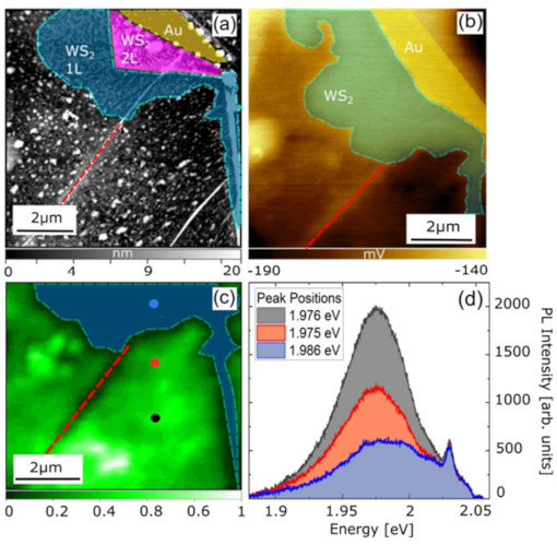
Optoelectronic Properties of Nanosystems
The optoelectronic properties of nanoscale systems such as carbon nanotubes (CNTs), graphene nanoribbons and transition metal dichalcogenides (TMDCs) are determined by their dielectric function. This complex, frequency dependent function is affected by excitonic resonances, charge transfer effects, doping, sample stress and strain, and surface roughness. Knowledge of the dielectric function grants access to a material’s transmissive and absorptive characteristics. In this study s-SNOM technology is used for extracting local dielectric variations. In addition, s-SNOM measurements were correlated with spatially resolved PL spectroscopy and KPFM measurements.
s-SNOM in correlation with local photoluminescence (PL) is a useful tool for identifying and characterizing interlayer excitons. This novel method opens also applications in low-dimensional systems like carbon nanotubes and graphene nanoribbons.
This measurement was realized with the IR-neaSCOPE+TERs.
Combined TERS and s-SNOM
Tip-enhanced Raman spectroscopy (TERS) and scattering-type scanning near-field optical microscopy (s-SNOM) enable optical imaging with a spatial resolution far below the diffraction limit of light. Although s-SNOM records the elastically scattered light (yielding information about the local refractive index and absorption), in TERS, the Raman scattered light is detected, which provides, for example, chemical information. Here, we introduce a combined TERS and s-SNOM setup for correlative studies of tip-enhanced elastically scattered and Raman scattered light. Comparing s-SNOM and TERS signals, we demonstrate a qualitative correlation between the tip-enhanced elastic and tip-enhanced Raman scattered light. Thus, recording the tip-enhanced elastically scattered light enables a fast and reliable TERS alignment. Further, we demonstrate experimentally and by simulations that Pt-coated silicon tips can be used for TERS in gap-mode configuration.
This unique technological marriage could be employed for correlative analyses of structural, chemical, and photonic sample properties.
This measurement was realized with the IR-neaSCOPE+TERs.
Organic Semiconductors
Semiconductors based on organic polymers have several advantages over their conventional, mostly silicon-based cousins. They are simpler and cheaper to manufacture, and can be produced in the form of thin, flexible layers, which allows them to be attached to diverse substrates and surfaces. Their electrical conductivity and energy efficiency are a function of the properties of the materials of which they are made. This degree of molecular order affects the mobility and transport of the charge carriers within them. Up until now, it has been very difficult to access these structures experimentally. s-SNOM and nano-FTIR make a valuable contribution to our understanding of these layered systems and to organic electronics in general.
s-SNOM & nano-FTIR is ideally suited for monitoring and optimize growth parameters to get highly ordered organic films and thus faster devices with crucial impact in development of optoelectronic devices such as OLED technology, or organic solar cells.
This measurement was realized with the IR-neaSCOPE+s.
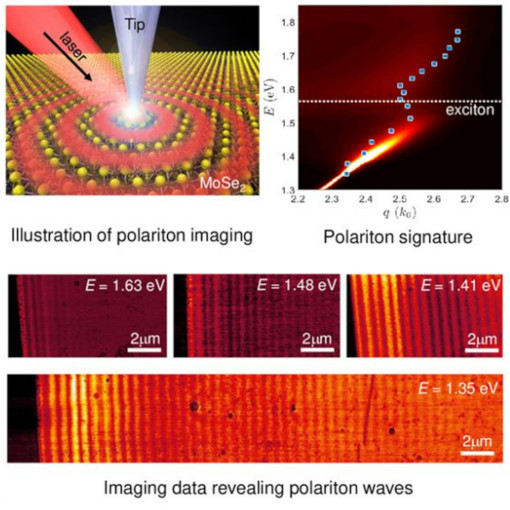
Exciton-Polaritons Propagation
The exciton–polariton (EP), a half-light and half-matter quasiparticle, is potentially an important element for future photonic and quantum technologies. It provides both strong light–matter interactions and long-distance propagation that is necessary for applications associated with energy or information transfer. Recently, strongly coupled cavity EPs at room temperature have been demonstrated in van der Waals materials due to their strongly bound excitons. Here, we report a nano-optical imaging study of waveguide EPs in MoSe2, a prototypical van der Waals semiconductor. The measured propagation length of the EPs is sensitive to the excitation photon energy and reaches over 12 µm. The polariton wavelength can be conveniently altered from 600 nm down to 300 nm by controlling the waveguide thickness. Furthermore, we found an intriguing back-bending polariton dispersion close to the exciton resonance. The observed EPs in van der Waals semiconductors could be useful in future nanophotonic circuits operating in the near-infrared to visible spectral regions.
This measurement was realized with the VIS-neaSCOPE+s.
Further reading:
Nanowerk News
Hu et al., Nature Photonics 11, 356 (2017)
Plasmon nanojet-based superlens
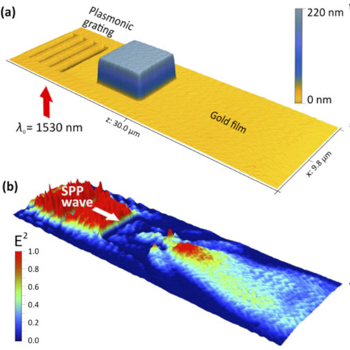
When a laser pulse of wavelength λ shines on the diffraction grating in the gold film, this gives rise to another type of electromagnetic excitations, known as surface plasmon polaritons. They propagate along the gold film and undergo 60% compression to a wavelength of 0.6λ when passing the square nanoparticle. This so-called plasmon nanojet effect, observed in the study for the first time, offers intriguing prospects for localizing light to the point where it becomes feasible to use it in fast and compact optical computers.
The authors proposed in this study a microstructure based on a dielectric cuboid placed on a thin metal film that can act as an efficient plasmonic lens allowing the focusing of surface plasmons at the subwavelength scale. Using numerical simulations of surface plasmon polariton (SPP) field intensity distributions, we observe high-intensity subwavelength spots and formation of the plasmonic nanojet (PJ) at the telecommunication wavelength of 1530 nm. The fabricated microstructure was characterized using amplitude and phase-resolved scattering-type scanning near-field optical microscopy. We show the first experimental observation of the PJ effect for the SPP waves. Such a novel, to the best of our knowledge, and simple platform can provide new pathways for plasmonics, high-resolution imaging, and biophotonics, as well as optical data storage.
This measurement was realized with the VIS-neaSCOPE+s.
Further reading:
News SciTechDaily
Minin et al., Optics Letters 45, 3244 (2020)
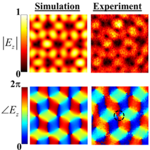
Optical Skyrmions
Best thought of as topological excitations that share the same topology as a set of magnetic moments wrapped around a sphere, skyrmions are widely thought to be promising for magnetic storage and spintronics applications. Shai Tsesses and colleagues have now brought skyrmions into the arena of optics. By controlling the interference of plasmon polaritons on a patterned metallic surface, they have succeeded in creating a lattice of optical skyrmions. The authors were able to image this pattern of evanescent electromagnetic fields using a phase-resolved near-field optical microscope. In contrast to their magnetic analogues studied in solid-state systems, these optical skyrmions can be continuously tuned from a so-called bubble- to Néel-type structure. However, in common with many such topological excitations, the lattice of optical skyrmions displays a remarkable robustness to imperfections.
The extent to which light can be manipulated and processed in photonic systems has already given us countess technologies. Few would bet against a few more popping out following this discovery of photonic skyrmions.
This measurement was realized with the VIS-neaSCOPE+s.
Excitations in Twisted Bilayer Graphene
Twisted bilayer graphene (TBG) can exhibit vastly different properties than those of single layers of graphene, especially when the two layers are rotated relative to each other by a small angle of approximately 1 degree. Investigating and probing these properties could be highly valuable, as it could ultimately enhance the current understanding of superconductivity and facilitate its use for the development of new devices. In this study s-SNOM investigation of TBG allows the spatial probing of interaction effects at the nanoscale and potentially elucidates the contribution of collective excitations to many-body ground states.
"As twisted graphene structures form a class of materials hosting many fascinating phenomena, we basically just have started the journey," says Prof. Koppens, the leader of the study. "We now aim to access the correlated states at cryogenic temperatures.
cryo s-SNOM technology sensitivity to the electronic properties of TBG could potentially point at the physical mechanisms of the superconducting and magnetic phenomena.
This measurement was realized with the cryo-neaSCOPE+xs.
Further reading:
News PHYS.ORG
Hesp et al., Nature Physics 17, 1162–1168 (2021)
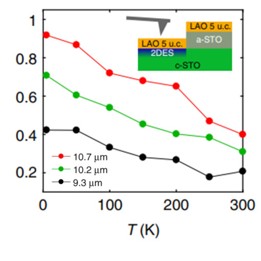
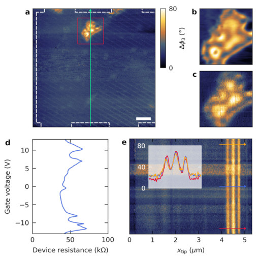
Conducting Oxide Interfaces
Probing the local transport properties of two-dimensional electron systems (2DES) confined at buried interfaces requires a non-invasive technique with a high spatial resolution operating in a broad temperature range. In this paper uses cryo s-SNOM as a tool for studying the conducting LaAlO3/SrTiO3 interface from room temperature down to 6º K. The s-SNOM signal, in particular its phase component, is highly sensitive to the transport properties of the electron system present at the interface.
cryo s-SNOM technology in combination with electrostatic gating provides novel application potential in phase separation and charge inhomogeneities due to ferroelectric domain walls, metal-insulator transitions and other emergent phenomena in a large family of 2D oxide interfaces.
This measurement was realized with the cryo-neaSCOPE+xs.
Further reading:
Luo et al., Nature Communications 10, 2774 (2019)
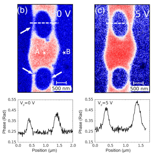
Electronic Transport in nano-Channels
Nanoscale channels realized at the conducting interface between LaAlO3 and SrTiO3 provide a perfect playground to explore the effect of dimensionality on the electronic properties of complex oxides. Here we compare the electric transport properties of devices realized using the AFM-writing technique and conventional photo-lithography. We find that the lateral size of the conducting paths has a strong effect on their transport behavior at low temperature. We observe a crossover from metallic to insulating regime occurring at about 50 K for channels narrower than 100 nm. The insulating upturn can be suppressed by the application of a positive backgate. We compare the behavior of nanometric constrictions in lithographically patterned channels with the result of model calculations and we conclude that the experimental observations are compatible with the physics of a quantum point contact.
cryo s-SNOM technology applies to oxide 2D nanoscale devices, confinement effects in future devices, and superconductivity.
This measurement was realized with the cryo-neaSCOPE+xs.
Further reading:
Boselli et al., Phys. Rev. B 103, 075431 (2021)
Social Distancing on the Nanoscale
Nanotechnology is already an integral part of modern electronics in our computers, smart phones or cars. The size of electronic components makes conventional optical microscopes no longer sufficient for inspecting these nanostructures. Therefore, scientists have replaced the optical microscope with much more sophisticated concepts, such as electron or scanning tunneling microscopy. However, these techniques use electrons instead of light, which can influence the properties of the nanoscale devices. Furthermore, these important measurement techniques are limited to electrically conducting samples. This study introduced a new technique, which can resolve electron motion on the nanoscale without needing to be electrically contacted. The concept behind the technique works similar to contactless payment, i.e. Near Field Communication (NFC). Better still, the new method also reaches unbelievable time resolution as good as one quadrillionth of a second (the femtosecond timescale).
Combining these extreme spatial and temporal resolutions makes the recording of slow-motion movies of ultrafast electron dynamics on the nanoscale possible.
This measurement was realized with the IR-neaSCOPE+fs.
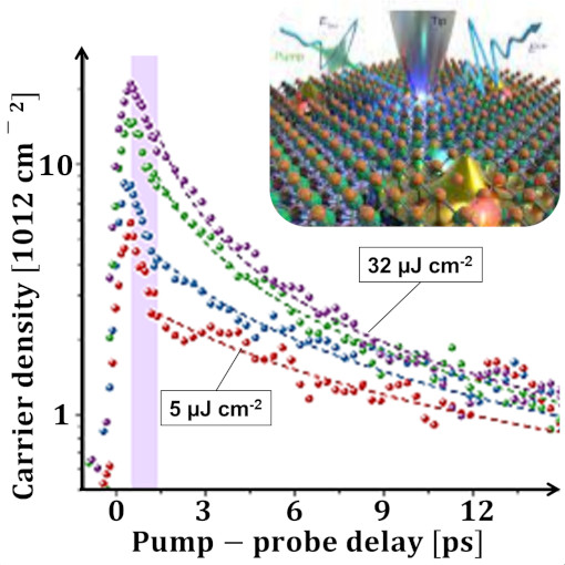
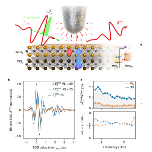
High-Density Exciton Phases
The density-driven transition of an exciton gas into an electron–hole plasma remains a compelling question in condensed matter physics. In two-dimensional transition metal dichalcogenides, strongly bound excitons can undergo this phase change after transient injection of electron–hole pairs. Unfortunately, unavoidable nanoscale inhomogeneity in these materials has impeded quantitative investigation into this elusive transition. This study demonstrates how ultrafast nanoscopy can capture the Mott transition through the density-dependent recombination dynamics of electron–hole pairs within a WSe2 homobilayer.
Ultrafast nanoscopy is a powerful technology to study strong electronic correlations and interlayer coupling within a diverse range of stacked and twisted 2D materials.
This measurement was realized with the IR-neaSCOPE+fs.
Further reading:
Siday et al., Nano Lett. (2022)
Electronic Motion in Nanowires
Modern nanotechnology aims to create artificial materials with novel properties, e.g. semiconductor nanowires for high-speed electronics. To understand the behavior of these structures and to make them even faster, smaller, and more efficient, scientists would like to trace directly how electrons move on length scales of only a few atoms. These processes often occur extremely quickly, which has spurred a drive to develop a microscope that combines excellent spatial resolution with the highest possible temporal resolution. This study trace the time-dependent dielectric function at the surface of a single photoexcited InAs nanowire in all three spatial dimensions.
Besides answering technological questions in electronics and photovoltaics, ultrafast pump-probe nanoscopy provides application potential ranging from novel physical insights into exotic materials to understanding biological processes on the molecular scale.
This measurement was realized with the IR-neaSCOPE+fs.
Further reading:
Eisele et al., Nature Photonics 8, 841–845 (2014)
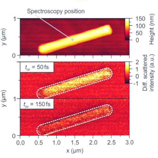
Electron Motion in Nanostructures
Charge transport in nanomaterials is the key process in many applications in nanoelectronics. An efficient tool for the characterization of charge transport in semiconductors nanostructures is terahertz (THz) spectroscopy, which involves contactless probing of the conductivity. Another more local investigation tool is THz s-SNOM which combines the THz frequencies with nanoscale resolution on an AFM. This study combines ultrafast pump-probe nanoscopy with THz s-SNOM which allow in-depth understanding of the nanoscale electron motion inside the nanobars. In addition, this study reveals that electrons are submitted to additional forces (band bending) close to the nanobar surfaces, which greatly enhance confinement of electrons at the picosecond timescale.
THz s-SNOM in combination with ultrafast pump-probe nanoscopy provides unique tool for the investigation of electron motion in nanostructure surfaces.
This measurement was realized with the THz-neaSCOPE+s.
Further reading:
Pushkarev et al., Advanced Functional Materials 5, (2022)
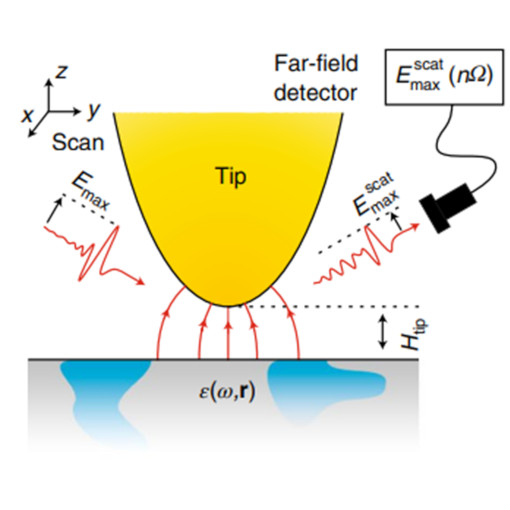
Nanoscale Terahertz Microscopy
Terahertz (THz) radiation has become an important diagnostic tool in the development of new technologies. However, the diffraction limit prevents terahertz radiation (λ ≈ 0.01–3 mm) from being focused to the nanometer length scale of modern devices. In response to this challenge, terahertz scanning probe microscopy techniques based on coupling terahertz radiation to subwavelength probes such as sharp tips have been developed. These probes enhance and confine the light, improving the spatial resolution of terahertz experiments by several orders of magnitude. In this Review, THz s-SNOM is compared with other probe microscopy techniques that achieve spatial resolution on the scale of micrometres to ångströms, with particular emphasis on their overarching approaches and underlying probing mechanisms.
THz s-SNOM provides unique and complementary information to conventional IR s-SNOM nanoscopy.
This measurement was realized with the THz-neaSCOPE+s.
Further reading:
Cocker et al., Nature Photonics 15, 558–569 (2021)
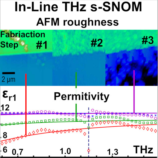
Coplanar Microwave Resonators
Superconducting quantum circuits are one of the leading quantum computing platforms. To advance superconducting quantum computing to a point of practical importance, it is critical to identify and address material imperfections that lead to decoherence. In this study THz s-SNOM probes the local dielectric properties and carrier concentrations of wetetched aluminum resonators on silicon, one of the most characteristic components of the superconducting quantum processors. We ?nd that the permittivity and carrier concentration of silicon in wetetched regions are modi?ed, leading to increased THz s-SNOM scattering compared to high-resistivity silicon. In conclusion, THz s-SNOM combines microscopy with local THz spectroscopy and can be used to identify processing-induced inhomogeneities that limit device function.
In-line THz nanoscopy is a non-invasive method to quantify and identify potential loss channels in quantum devices without the need of electrical contacts.
This measurement was realized with the THz-neaSCOPE+s.
Further reading:
Guo et al., Appl. Phys. Lett. 119, 091101 (2021)
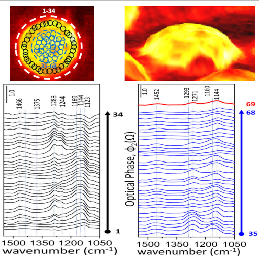
Enzymatical Biocatalytic Reactions
Biocatalytic transformations in living organisms, such as multi-enzyme catalytic cascades, proceed in different cellular membrane-compartmentalized organelles with high efficiency. Nevertheless, it remains challenging to mimic biocatalytic cascade processes of natural systems. One method to mimic natural enzymes is the use of multi-shelled metal-organic frameworks (MOFs). Such MOFs can be used as a hierarchical scaffold to spatially organize enzymes on nanoscale to enhance cascade catalytic efficiency. In this study, the authors employed s-SNOM and nano-FTIR technology, which resolves nanoscale heterogeneity of vibrational activity associated to enzymes encapsulated in multi-shelled MOFs. This work provides important insights into developing complex multi-spatial compartmental systems for multi-enzyme catalytic cascades that hold great promise in many industrial processes.
Infrared nanoscale analysis reveals molecular identity of nm-small materials. Method which can be applied in many chemical and pharmaceutical industrial processes.
This measurement was realized with the IR-neaSCOPE+s.
Further reading:
Man et al., Nature Communications 13, 305 (2022)
Phonon Polaritons & Organic Molecules
Light plays an essential role in modern science and technology, with applications ranging from fast optical communication to medical diagnosis and laser surgery. In many of these applications, the interaction of light with matter is of fundamental importance. The images obtained in this work reveal that the interaction between infrared light and molecular vibrations can be so strong that eventually the material properties are modified, such as conductivity and chemical reactivity. This effect, called vibrational strong coupling, could be used in the future for development of ultrasensitive spectroscopy devices or to study quantum aspects of strong vibrational coupling that have been not accessible so far.
Infrared s-SNOM imaging reveals vibrational strong coupling between propagating phonon polaritons and small organic molecules. A phenomenon with high potential to control fundamental physical and chemical material properties.
This measurement was realized with the IR-neaSCOPE+s.
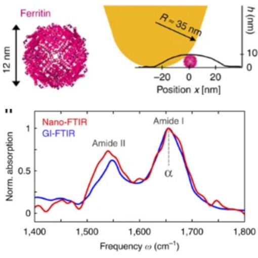
Secondary Structure of Single Proteins
The secondary structure of a proteins is highly relevant in the pathogenous mechanism leading to Alzheimer, Parkinson, and other neuro-degenerative diseases. Although a variety of methods have been developed to study the protein chemistry and structure, recognizing and mapping the secondary structure on the nanometer scale, or even with single protein sensitivity, is still a major challenge. nano-FTIR technology is used in this study to enabled nanoscale chemical imaging and probing of protein’s secondary structure with enormous sensitivity. In short, a sharp metalized tip is illuminated with a broadband infrared laser beam, and the backscattered light is analyzed with a specially designed Fourier transform spectrometer.
nano-FTIR probes the infrared spectroscopy and resolves the secondary structure of proteins complexes with diameter of 12 nm, 6 nm protein monolayer and even of 3 nm thin fibrils.
This measurement was realized with the IR-neaSCOPE+s.
Further reading:
Amenabar et al., Nature Communications 4, 2890 (2013)
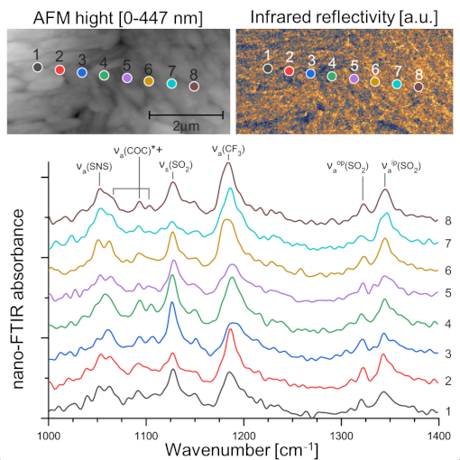
E-Book on Polymer Nanostructures
Nanocomposite polymers, multilayer thin films, nanofibers and other polymer nanoforms often offer new properties or enhanced performance compared to bulk materials, demanding tools for chemical analysis with nanoscale spatial resolution for their investigations. We introduce in this e-book leading techniques for nanoscale chemical mapping and identification.
Applications covered in this e-book:
- Nanoscale chemical identification using standard IR database,
- IR nanoimaging of polymer films, nanoparticles & monolayers,
- Molecular conformation and orientation in an ultrathin polymer film,
- Hyperspectral & correlative nanoscopy of polymer composites.
This measurement was realized with the IR-neaSCOPE.
Further reading:
E-Book Download
Flexible Organic Photovoltaics
Organic photovoltaics hold great potential for cost-effective, sustainable and flexible devices production. On the other side, organic semiconductor films are semicrystalline material with energetic disorder, inefficient carrier transport and high energy loss. Several studies focused on morphology strategy proposed the development of better suited phase separation to improved structure order, facilitate efficient transport and suppress trap states. This report uses tapping AFM-IR+ to map mixtures of organic photovoltaic blends and fine-tune the material morphology and crystallization. The Authors concludes that mixtures of blends with structural similarity but with different electronic properties exhibit significant improvement of high-crystallinity, fibrillar morphology and even shows enhancement in performance.
In contrast to electrons, IR photons extends the structural investigation beyond the top atomic layer complementing current nanoscale investigation methodology. Therefore, the IR-based investigation methods (AFM-IR, s-SNOM and nano-FTIR) can be also applied to other thin-film materials, e.g. sensors, electronic equipments or semiconductor devices.
This measurement was realized with the IR-neaSCOPE.
Further reading:
Zhang et al., Advanced Materials 33, 2007177 (2021)
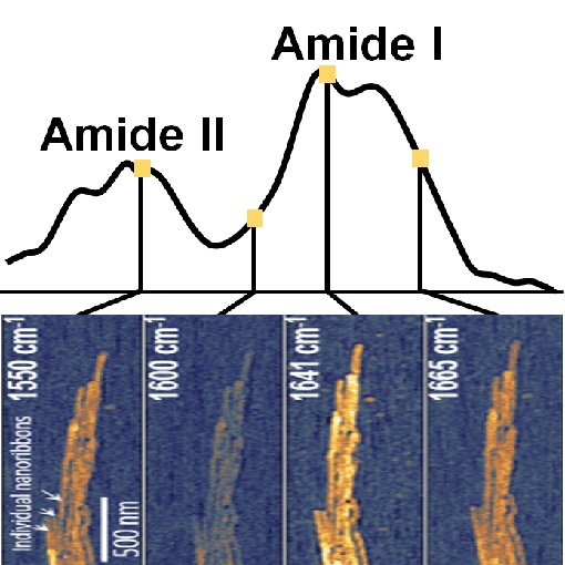
Mineralization of Protein Nanoribbons
Dental enamel is the hardest tissue created by vertebrates and exhibits complex nanoscale organizations of apatite crystals and protein nanoribbons. Previous studies using AFM and TEM show the formation of nanoribbons and even suggested their twisted structure. In this study, tapping AFM-IR+ provides additional chemically-specific information by measuring local infrared sample absorption. And indeed, absorption in the amide I and amide II bands verifies the protein composition of nanoribbons and provides insights into their α-helix/β-turn secondary structure. In addition to basic understanding of enamel growth, this study it is an important step towards synthesis of nanostructured materials using self-assembled organic framework.
Using low energy photons, tapping AFM-IR+ is highly suitable for nanoscale imaging and spectroscopy of fragile biological samples, such as protein, fibrils, lipids, viruses and DNA.
This measurement was realized with the IR-neaSCOPE.
Further reading:
Bai et al., PNAS 117, 19201-19208 (2020)