


Interface nano-Electrochemistry Study
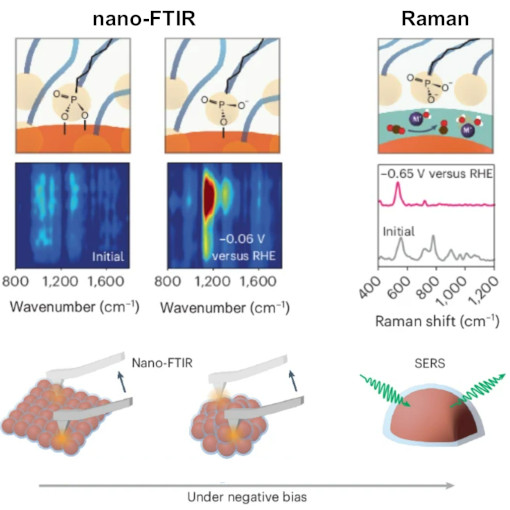
Recent advancements in nanocatalysis have been significantly bolstered by the application of nano-FTIR (infrared nanospectroscopy) and surface-enhanced Raman spectroscopy (SERS), providing unprecedented insights at the molecular level. nano-FTIR, especially valuable due to its high spatial resolution, has elucidated the electrochemically driven transformation of ligands on nanoparticles, which is crucial for creating active microenvironments for reactions like CO2 to CO conversion. This transformation involves the detachment and reconfiguration of ligands, a process dynamically captured through the concurrent use of nano-FTIR and SERS. The integration of these techniques allows for a detailed observation of ligand dynamics and the formation of an electrocatalytic interlayer, highlighting the importance of precise molecular arrangement for enhancing catalytic efficiency.
nano-FTIR, when combined with Raman spectroscopy, underscores the pivotal role of controlled ligand behavior in steering the selectivity and activity of nanocatalytic processes.
This measurement was realized with the IR-neaSCOPE+TERs.
Further reading:
Yu et al., Nature Catalysis 2380, 9 (2024)
Nano-Interface 2D Alloys
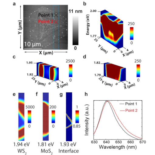
Single-layer heterostructures exhibit striking quasiparticle properties and many-body interaction effects that hold promise for a range of applications. However, their properties can be altered by intrinsic and extrinsic defects, thus diminishing their applicability. Therefore, it is of paramount importance to identify defects and understand 2D materials’ degradation over time using advanced multimodal imaging techniques. Here we implemented a liquid-phase precursor approach to synthesize 2D in-plane MoS2–WS2 heterostructures exhibiting nanoscale alloyed interfaces and map exotic interface effects during photodegradation using a combination of hyperspectral tip-enhanced photoluminescence and Raman and near-field nanoscopy. Surprisingly, 2D alloyed regions exhibit thermal and photodegradation stability providing protection against oxidation. Coupled with surface and interface strain, 2D alloy regions create stable localized potential wells that concentrate excitonic species via a charge carrier funneling effect. These results demonstrate that 2D alloys can withstand extreme degradation effects over time and could enable stable 2D device engineering.
This measurement was realized with the IR-neaSCOPE+TERs.
Optoelectronic Properties of Nanosystems
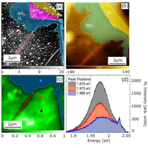
The optoelectronic properties of nanoscale systems such as carbon nanotubes (CNTs), graphene nanoribbons and transition metal dichalcogenides (TMDCs) are determined by their dielectric function. This complex, frequency dependent function is affected by excitonic resonances, charge transfer effects, doping, sample stress and strain, and surface roughness. Knowledge of the dielectric function grants access to a material’s transmissive and absorptive characteristics. In this study s-SNOM technology is used for extracting local dielectric variations. In addition, s-SNOM measurements were correlated with spatially resolved PL spectroscopy and KPFM measurements.
s-SNOM in correlation with local photoluminescence (PL) is a useful tool for identifying and characterizing interlayer excitons. This novel method opens also applications in low-dimensional systems like carbon nanotubes and graphene nanoribbons.
This measurement was realized with the IR-neaSCOPE+TERs.
Combined TERS and s-SNOM
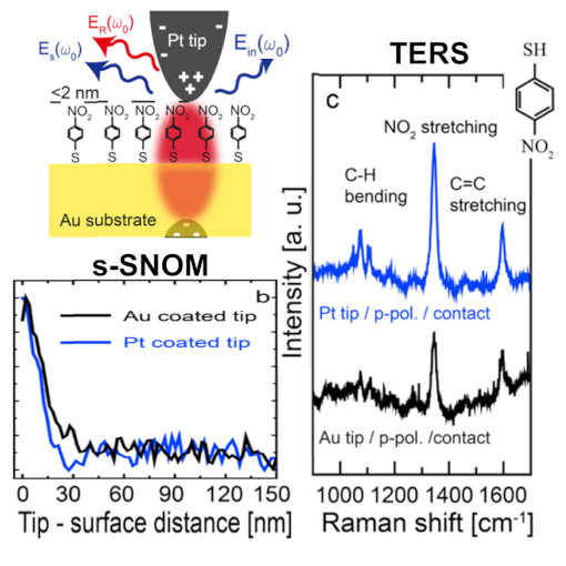
Tip-enhanced Raman spectroscopy (TERS) and scattering-type scanning near-field optical microscopy (s-SNOM) enable optical imaging with a spatial resolution far below the diffraction limit of light. Although s-SNOM records the elastically scattered light (yielding information about the local refractive index and absorption), in TERS, the Raman scattered light is detected, which provides, for example, chemical information. Here, we introduce a combined TERS and s-SNOM setup for correlative studies of tip-enhanced elastically scattered and Raman scattered light. Comparing s-SNOM and TERS signals, we demonstrate a qualitative correlation between the tip-enhanced elastic and tip-enhanced Raman scattered light. Thus, recording the tip-enhanced elastically scattered light enables a fast and reliable TERS alignment. Further, we demonstrate experimentally and by simulations that Pt-coated silicon tips can be used for TERS in gap-mode configuration.
This unique technological marriage could be employed for correlative analyses of structural, chemical, and photonic sample properties.
This measurement was realized with the IR-neaSCOPE+TERs.