

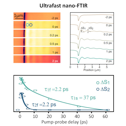
Plasmons Revolutionize Optoelectronics
In recent developments, researchers from multiple prestigious institutions across China have significantly advanced optoelectronics by harnessing the properties of hyperbolic transient plasmons in black phosphorus (BP), a material known for its unique anisotropic electronic and optical characteristics. This advancement comes from the ability to manipulate BP's charge carriers, enabling hyperbolic plasmon polaritons and overcoming previous challenges associated with hyperbolic polariton materials. The breakthrough involved a topological transition in BP's dielectric tensors through photo-induced carrier injection, making it possible to transform its iso-frequency contour and unlock the potential of rare transient hyperbolic plasmons. These plasmons exhibit ultrafast transitions, minimal propagation losses, and efficient optical emissions.The ultrafast nano-FTIR nanoscopy technique has been pivotal in revealing transient plasmonic phenomena at the nanoscale, driving innovations in optoelectronics, photonic circuits, sensors, and energy systems through the dynamic modulation of BP's properties.
This measurement was realized with the IR-neaSCOPE+fs.
Further reading:
Fu et al., Nature Communications 15, 709 (2024)
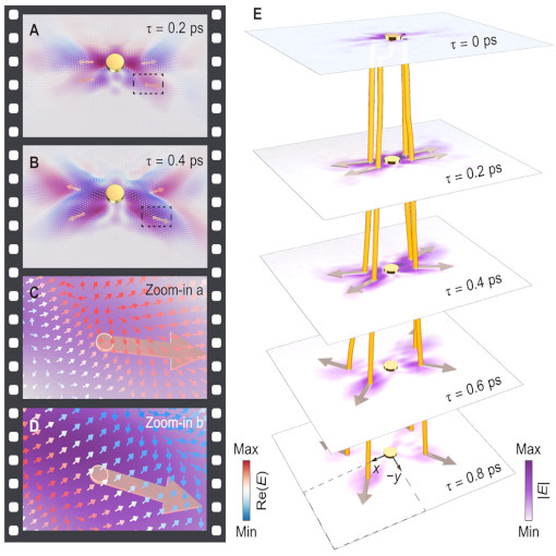
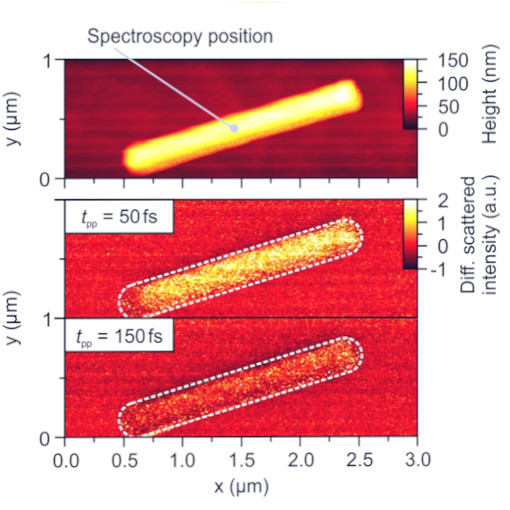
Unveiling Polariton Pulse Dynamics
This study explores polariton pulses - unique light-matter waves - and their complex behaviors in anisotropic media, driven by ultrafast and minuscule field changes. Using innovative time-resolved nanoimaging and advanced data processing, researchers have unveiled fascinating spatiotemporal dynamics, like curved energy flows and differing wave and energy velocities.The paper highlights the inadequacies of current technologies in capturing these rapid, directional, and nanoscale phenomena. The breakthrough nano-FTIR technology overcomes these limitations, enabling detailed visualization and analysis of polariton pulse behaviors. This advancement paves the way for transformative developments in ultrafast nanoimaging, with implications for molecular sensing, hyperlensing, and nanophotonic energy control.In summary, this research opens new horizons in optics and material science, from investigating intricate space-time dynamics at unprecedented scales to advancing ultrafast nanoimaging, marking a significant leap in the field.
This measurement was realized with the IR-neaSCOPE+fs.
Further reading:
Zhang et al., Science Advances 9, eadi4407 (2023)
Social Distancing on the Nanoscale
Nanotechnology is already an integral part of modern electronics in our computers, smart phones or cars. The size of electronic components makes conventional optical microscopes no longer sufficient for inspecting these nanostructures. Therefore, scientists have replaced the optical microscope with much more sophisticated concepts, such as electron or scanning tunneling microscopy. However, these techniques use electrons instead of light, which can influence the properties of the nanoscale devices. Furthermore, these important measurement techniques are limited to electrically conducting samples. This study introduced a new technique, which can resolve electron motion on the nanoscale without needing to be electrically contacted. The concept behind the technique works similar to contactless payment, i.e. Near Field Communication (NFC). Better still, the new method also reaches unbelievable time resolution as good as one quadrillionth of a second (the femtosecond timescale).
Combining these extreme spatial and temporal resolutions makes the recording of slow-motion movies of ultrafast electron dynamics on the nanoscale possible.
This measurement was realized with the IR-neaSCOPE+fs.
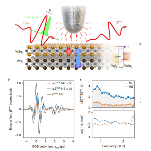
High-Density Exciton Phases
The density-driven transition of an exciton gas into an electron–hole plasma remains a compelling question in condensed matter physics. In two-dimensional transition metal dichalcogenides, strongly bound excitons can undergo this phase change after transient injection of electron–hole pairs. Unfortunately, unavoidable nanoscale inhomogeneity in these materials has impeded quantitative investigation into this elusive transition. This study demonstrates how ultrafast nanoscopy can capture the Mott transition through the density-dependent recombination dynamics of electron–hole pairs within a WSe2 homobilayer.
Ultrafast nanoscopy is a powerful technology to study strong electronic correlations and interlayer coupling within a diverse range of stacked and twisted 2D materials.
This measurement was realized with the IR-neaSCOPE+fs.
Further reading:
Siday et al., Nano Lett. (2022)
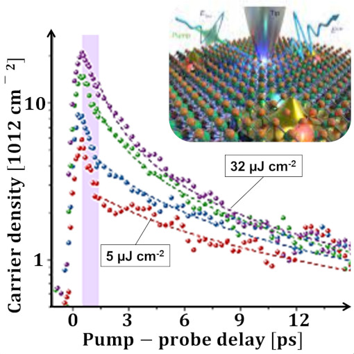
Electronic Motion in Nanowires
Modern nanotechnology aims to create artificial materials with novel properties, e.g. semiconductor nanowires for high-speed electronics. To understand the behavior of these structures and to make them even faster, smaller, and more efficient, scientists would like to trace directly how electrons move on length scales of only a few atoms. These processes often occur extremely quickly, which has spurred a drive to develop a microscope that combines excellent spatial resolution with the highest possible temporal resolution. This study trace the time-dependent dielectric function at the surface of a single photoexcited InAs nanowire in all three spatial dimensions.
Besides answering technological questions in electronics and photovoltaics, ultrafast pump-probe nanoscopy provides application potential ranging from novel physical insights into exotic materials to understanding biological processes on the molecular scale.
This measurement was realized with the IR-neaSCOPE+fs.
Further reading:
Eisele et al., Nature Photonics 8, 841–845 (2014)