
Scanning Gate Microscopy (SGM)
SGM utilizes the ability of an AFM tip to influence the electrostatic properties of a sample locally. By applying voltage to the scanning tip, the tip acts as a movable electrical gate that can modify electrostatic potential for electrons in the sample and thus enables exploring electronic and transport properties at the nanoscale (Figure 1).
This approach has already been proven useful at temperatures > 4K in e.g. imaging current flow through quantum point contacts [M.P. Jura et al., Nature Phys. 3, 841 (2007)], or in visualizing coherent transport and universal conductance fluctuations in graphene [J. Berezovsky et al., Nanotechnology 21, 274013 (2010)]. By adopting SGM to mK temperatures, quantum phenonema can be probed since electron mobilities further increase along with thermal fluctuations further decreasing, which is the prerequisite for reaching the necessary energy resolution.
Tuning-fork-based AFMs with wire-type tips are better suited for SGM than cantilever-based AFMs, since the cantilever strongly influences the capacitive coupling between tip and sample, and hence washes out the localization of the tip potential.
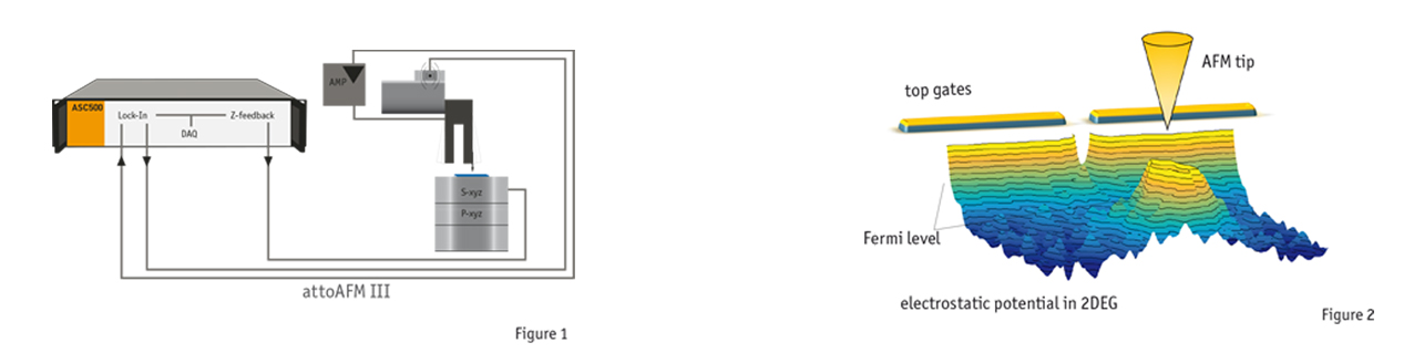
The attoAFM III is the perfect microscope platform for electrical transport measurements on the nanoscale. Figure 2: A typical potential landscape for a scanning gate experiment on a GaAs/AlGaAs heterostructure. It demonstrates the size of the tip-induced potential as well as the influence of the disorder potential (image courtesy of R. Steinacher, ETH Zurich, Switzerland).