
Kelvin Probe Force Microscopy (KPFM)
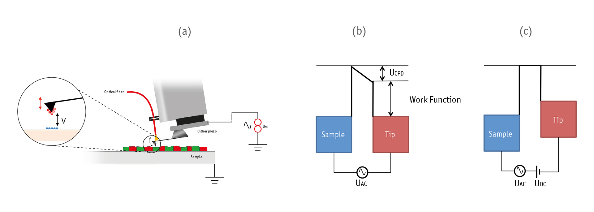
Kelvin Probe Force Microscopy (KPFM), also known as Surface Potential Microscopy, is a non-contact mode AFM technique capable of imaging local variations in the Work Function of a sample (see Figure a). The work function is defined as the binding energy of the outermost electron of a given material with regards to the vacuum level. Since KPFM uses a probe (AFM tip) with its own work function, overlapping with the sample’s work function (see Figure b), KPFM yields information about the difference between the two, called contact potential difference (UCPD).
To model the KPFM geometry for quantification of the results, one can think of the AFM tip and the sample as two sides of a capacitor. The force between these sides can be expressed as F = 1/2 dC/dz U2, where C is the effective capacitance and U is the total potential difference between the sample and tip. This difference U can be split up in two terms:
i) The first term is the Contact Potential Difference (UCPD); as mentioned above, this is the difference between the work function of tip and sample (Figure b).
ii) The second term is the additional voltage that is applied to the tip relative to the sample. Typically, one applies a DC voltage as well as a AC component with frequency ω. This potential is hence written as Uext = UDC + UAC sin(ωt).
Substituting U = UCPD +Uext in the force expression above allows us to calculate the electrostatic force acting on the tip. Among other terms, one component Fω is proportional to sin(ωt): Fω= dC/dz [UDC − UCPD] UAC sin(ωt). This term vanishes when UDC equals UCPD (see Figure c). So, modifying the DC voltage until the force is zero allows to measure the contact potential difference. To achieve this, Fω simply needs to be recorded using a lock-in amplifier. Its output can then be used for a feedback that tries to modify UDC so that the vibration amplitude is zero. This is the measurement scheme behind a Kelvin Probe Measurement: to always adjust UDC so, that the force on the tip and therefore its vibration at frequency ω are zero.
By recording the applied UDC, one can image the Contact Potential Difference directly, and hence one is able to extract nanoscale spatial information about work function variations of the sample.
Kelvin Probe Force Microscopy has wide spread use in many different areas of surface science. In case of semiconductors it allows to investigate local electrical potentials and band bending distribution. It can image the electrical properties of metallic nanostructures, and help to investigate the local charge transfer of catalyst nanostructures for example.