Conducting-tip Atomic Force Microscopy (ct-AFM)
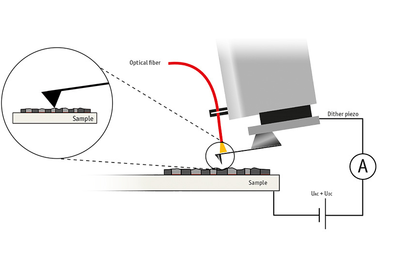
Conducting/conductive-tip atomic force microscopy is another variant of AFM, which uses conductive cantilevers and a bias voltage on the sample to measure the resulting current through the tip and sample interface. As the tip is in contact with the sample only locally, the measured resistance is dominated by the local resistance of the sample. Typically, the tip is brought into contact with the sample surface, and then scanned across it with a bias voltage applied. During the scan, the current is measured with the help of a low-noise and sensitive current amplifier. In order to improve the sensitivity, a lock-in can also be employed for this type of measurement. Current-voltage characteristics (I-V curves) can also be acquired either in DC mode, or dI-dV curves with a bias voltage and an additional AC probing voltage on top of it.
This latter mode is used in the so-called path or grid mode with the ASC500 SPM controller to acquire such local spectra at pre-defined local positions within the available scan area.
Depending on the local sample structure, as well as on the surface quality, this reveals local differences in sample conductivity on the nanoscale. In certain conditions, ct-AFM is similar to scanning tunneling microscopy. Thin oxide layers can act as tunnel barriers. Since the tunneling current is extremely sensitive to the oxide thickness, this leads to an exponential dependence of the current on the oxide thickness. This leads to images governed by few isolated spikes that correspond to the places with the thinnest oxide layer (log-normal distribution of current amplitudes).

