

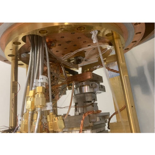
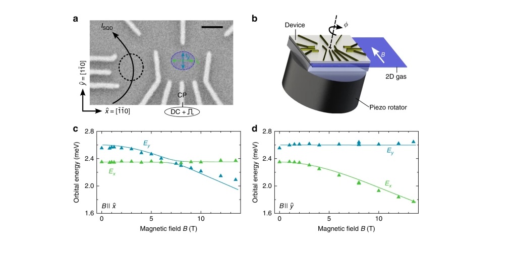
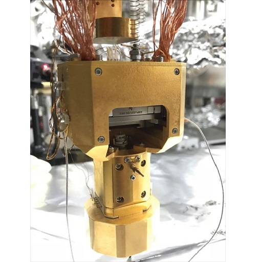
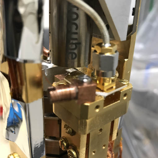
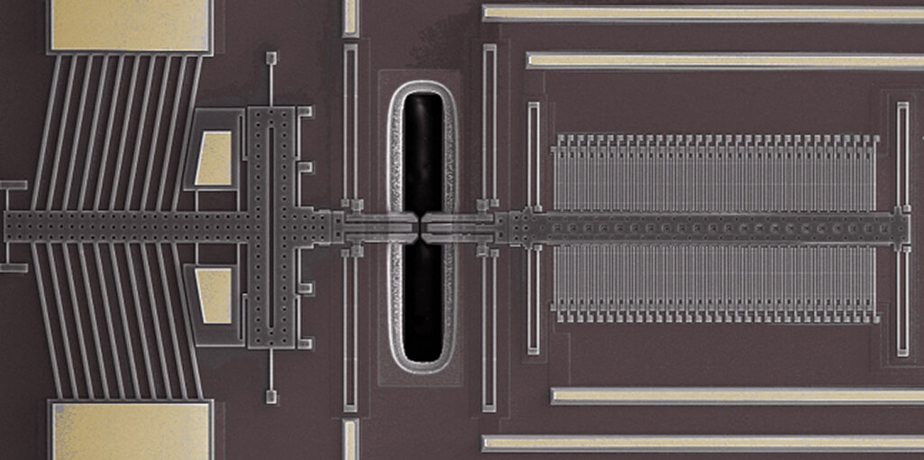
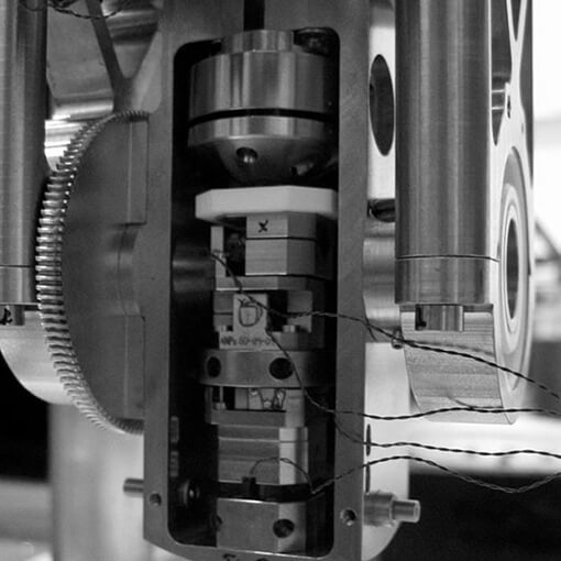
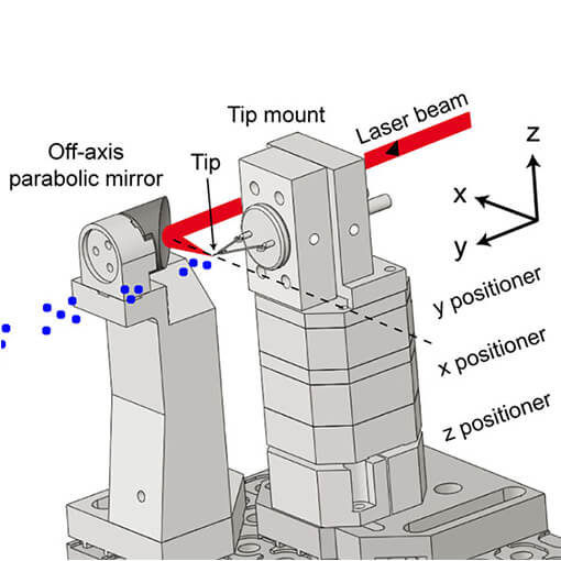
Unparalleled photon number resolution
While many breakthroughs in quantum optics have been carried out on the shoulders of single photon detectors, the group of Hong Tang (Yale University, USA) has only recently ramped up the game with a high-speed-response 100-pixel photon-number-resolving detector. This on-chip detector is moved precisely by attocube ANP positioners to make the electrode contact with a multi-channel RF probe, as well as to align the fiber array to grating couplers at cryogenic temperatures.
By spatiotemporally multiplexing an array of superconducting nanowires along a single waveguide, it is possible to observe the quantum photon statistics of a true thermal light source for the first time.
This result opens new paths for photonic quantum computation and quantum metrology.
This measurement was realized with the ANPz101/LT - linear z-nanopositioner, and the ANPx341/LT - linear x-nanopositioner.
Further reading:
R. Cheng et al., Nature Photonics 17, 112 (2023)
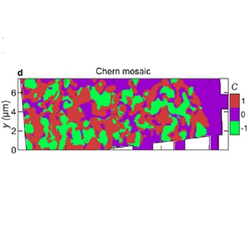
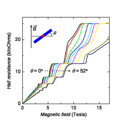
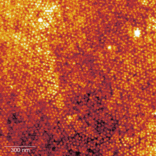
Imaging Chern mosaic and Berry-curvChern Mosaic in magic angle graphene
Graphene is still offering plenty of not yet fully understood phenomena to investigate. Influence on transport and magnetic properties of the itinerant electrons in magic-angle graphene is one of them. The scientists lead by Eli Zeldov (Weizmann Institute, IL) are investigating multiple factors, with their SQUID on a tip, built on attocubes ANP positioners, of which one is Chern mosaic. The measurements show paramagnetic-like patches (green) and diamagnetic-like patches (red), which are not easily explained according to the desire to minimize magnetic energy. Two mechanisms are proposed, which will need more investigation. The first mechanism depends on Hartree-Fock calculations, suggesting the system may break the sublattice symmetry spontaneously near ν = 1, even in the absence of an external sublattice potential.
To know more about the second possible mechanism and other findings you can read the article in Nature Physics:
This measurement was realized with the ANPx101/LT - linear x-nanopositioner.
Further reading:
S. Grover et al., Nature Physics 18, 885 (2022)
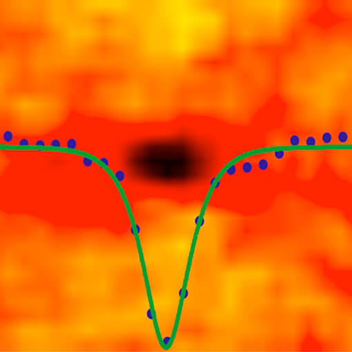
Anomalous vortex dynamics in URu2Si2
Uranium ruthenium silicide (URu2Si2) is an interesting superconductor but despite the attention it has been getting in recent condensed matter science, some of its properties are still quite controversial.
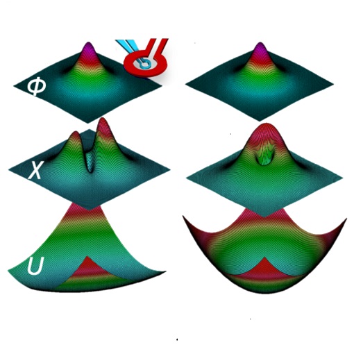
The scientists lead by Kathryn Moler (Stanford University, USA) have been using their sSQUID microscope, based on attocube ANP positioners, for measurements of spontaneous magnetism, rotational symmetry of lattice structures, and superconducting gap structures. The figure schematically shows the values of local flux Φ and local ac susceptibility χ expected for an isolated vortex for anisotropic (left) and isotropic (right) vortex pinning potentials U. These and their other measurements performed on URu2Si2 indicate a nodal gap structure and that chiral superconductivity either is not present or does not lead to detectable spontaneous magnetization.
This measurement was realized with the ANPx101/LT - linear x-nanopositioner.
Further reading:
Y. Iguchi et al., Phys. Rev. B 103, L220503 (2021)
Moiré Chern insulator for magnetic memories
In spin torque-based magnetic memories, magnetic bits can be switched using electrically-driven spin currents. The team lead by Andrea Young (University of California at Santa Barbara, USA) in collaboration with the group of Kin Fai Mak and Jie Shan (Cornell University, USA) has studied AB-stacked MoTe2/WSe2. This intriguing system showcases a remarkable accumulation of strong Berry curvature (BC) near the edges of the Hubbard band, resulting in a ubiquitous Spin Hall effect and a well-formed Chern insulator state at half filling of the moiré unit cell. Employing a nanoSQUID setup equipped with attocube nanopositioners (ANPx101, ANPz102) and scanners (ANSxy100), the team directly imaged the interplay between these two effects manifesting in ultra-low current magnetization switching within a singular system - a highly sought-after capability for efficient magnetic memory bits.
This measurement was realized with the ANPx101/RES/LT/HV - linear x-nanopositioner, and the ANPz101/RES/LT/HV - linear z-nanopositioner.
Further reading:
C. L. Tschirhart et al., Nature Physics 19, 807 (2023)
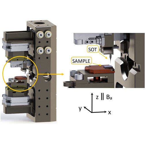
Mastering quantum computing via magnetic imaging with quantum probes
One of the most promising realizations of quantum computer relies on circuits of superconducting qubits. In order to come up with the optimal design of such circuits, physicists need to trace the paths of electrical currents. This can be done through monitoring the magnetic fields produced by the currents according to the Ampère´s law.
The team lead by Martino Poggio (University of Basel & Swiss Nanoscience Institute, Switzerland), in collaboration with the group of Andreas Wallraff (ETH Zurich, Switzerland), has imaged magnetic fields of a superconducting qubit circuit by scanning microscopy utilizing SQUID-on-tip (SOT) as the probe. In their experimental setup they used attocube cryogenic nanopositioners (ANPx311/LT/HV) and scanners (ANSxy100lr/LT/HV) at 4 K. Their method precisely detects both positive and negative effects of qubit couplings, making it instrumental in designing circuits with low qubit decoherence, which is a prerequisite for increased quantum computing efficiency.
This measurement was realized with the ANSxy100lr/LT/HV xy-Scanner made from Titanium, and the ANPx311/LT/HV - linear x-nanopositioner.
Further reading:
E. Marchiori et al., Appl. Phys. Lett. 121, 052601 (2022)
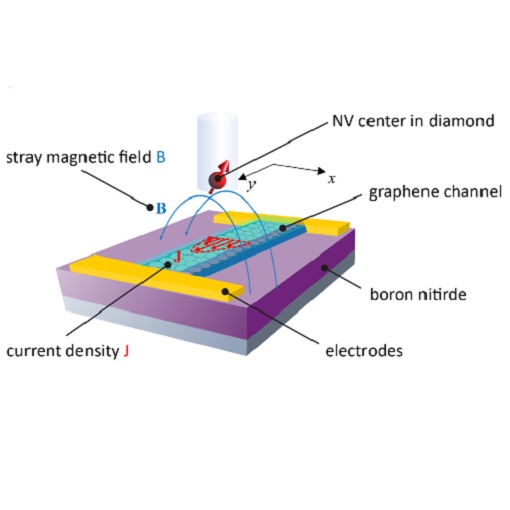
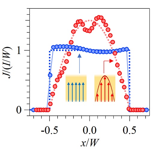
Viscous Dirac fluid paparazzied by NV magnetometry
Electronic transport in strongly-correlated quantum materials can involve substantial complexity that defy conventional description. An example of novel transport phenomenon that can arise in quantum materials is the collective movement of electrons reminiscent of that of a hydrodynamic fluid, in which viscosity can lead to non-uniform, parabolic current profile known as Poiseiulle flow. The electron-hole plasma in graphene at the charge neutrality point, known as the Dirac fluid, has been theoretically predicted as a candidate for such behavior. The team lead by Ronald Walsworth (prev. Harvard University, USA, now University of Maryland, USA) and Amir Yacoby (Harvard University, USA) established the existence of viscous Dirac-fluid flow in graphene by imaging the magnetic stray field associated with the electron flow. Imaging has been conducted by nitrogen vacancy magnetometry (NVM) in a setup comprising attocube nanopositioners ANP101 and ANS100. Single-spin scanning NVM, complemented by wide-field NVM imaging, reveals a parabolic Poiseuille profile, which is a characteristic of viscous transport, and in contrast with the uniform flow profile of conventional Ohmic conductors. Their results render NVM a suitable tool for probing the behavior of correlated electrons at the nanoscale.
This measurement was realized with the ANSxyz100std/LT xyz-Scanner made from Titanium, and the ANPx101/RES/LT/HV - linear x-nanopositioner.
Further reading:
M.J.H. Ku et al., Nature 583, 537 (2020)
3D tunable cavity in ultra low-vibration closed cycle cryostat
Experimental quantum optics is based on controlling the light-matter interaction. This work presents an open Fabry-Pérot cavity optical resonator giving the possibility to locate the region of interest on a solid-state sample as well as in-situ tuning of the cavity degrees of freedom.
In a joint project between an internal research team at attocube and Nanophotonics group of Alexander Högele (Ludwig Maximilian University of Munich, Germany) an open-cavity is realized inside a closed loop attoDRY800 cryostat with precise manipulations using ANPxyz positioners. Tremendous work put into a combination of passive and active vibration damping techniques allow the system to reach an exceptional level of mechanical stability. The researchers have demonstrated the formation of exciton-polaritons in this open-cavity platform with two-dimensional semiconductor and cavity photons as a hallmark of strong light-matter coupling.
The results establish the concept of an open-cavity in a closed-cycle cryostat as a promising quantum hardware tool to advance the field of solid-state quantum optics and cavity quantum electrodynamics.
This measurement was realized with the ANPx101/RES/LT - linear x-nanopositioner, the ANPz101/RES/LT - linear z-nanopositioner, the ANPx311/RES/LT - linear x-nanopositioner, and the attoDRY800.
Further reading:
S. Vadia et al., PRX Quantum 2, 040318 (2021)
Towards quantum internet
The team of Paul Barclay (University of Calgary, Canada) has been shaping the field of cavity optomechanics. Their most recent breakthrough is a demonstration of an interface between light and qubit, that utilizes the susceptibility of spin qubits to strain. They control spins of nitrogen-vacancy centers in diamond with telecom-wavelength photons. This novel approach gives more flexibility in the choice of spin qubit for the design of a quantum network as it does not require perfect spin-photon interface. Using standard telecom wavelength makes it not only suitable for long distance fiber-based networks but could also open the capability of connecting into existing technology. In the core of this new setup is a diamond microdisc resonator between the qubit and the light, sitting on top of an attocube positioner stack with the ANSxyz100 scanner for sub-nm positioning resolution.Read the full article in Nature Physics here:
This measurement was realized with the ANSxyz100std/LT xyz-Scanner made from Titanium.
Further reading:
P.K. Shandilya et al., Nature Physics 17, 1420 (2021)
Tunable microcavity as highly efficient single-photon source
The quest for ideal single photon sources is definitely on, as they would be instrumental in enabling quantum communication and quantum computing on a large scale. As strict requirements on the efficiency of single-photon creation in such applications have seldomly been met up to now, the realization of this route towards quantum future was somewhat hindered. By tuning an open microcavity, the group of Richard Warburton (University of Basel, Switzerland) has generated a highly efficient source of single photons from quantum dots that can operate with GHz repetition rate, while maintaining excellent single photon purity and indistinguishability. They managed to more than double the previous record on efficiency. The tunability of microcavity has been achieved by utilizing two sets of cryogenic nanopositioners: one that enables full in situ spatial (xy) and spectral (z) tuning of the microcavity (2x ANPx51, 1x ANPz51), and the other one that ensures a proper positioning of the microcavity with respect to the objective lens (2x ANPx101, 1x ANPz101).
This measurement was realized with the ANPx101/LT - linear x-nanopositioner, the ANPz101/LT - linear z-nanopositioner, the ANPx51/LT - linear x-nanopositioner, and the ANPz51/LT - linear z-nanopositioner.
Further reading:
N. Tomm et al., Nature Nanotechnol. 16, 399 (2021)
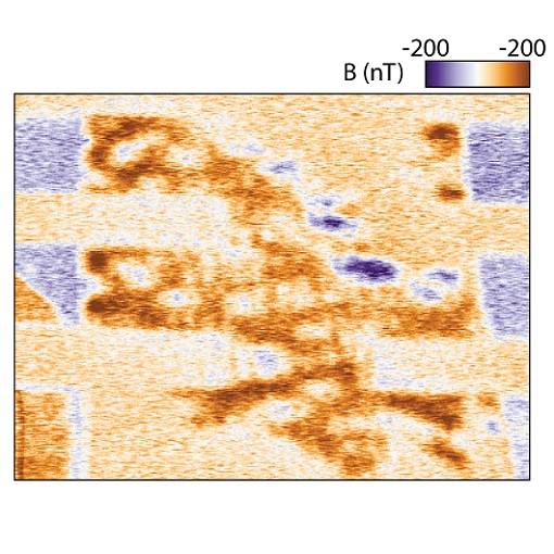
Long-range nontopological edge currents in graphene
In search for novel and exotic transport phenomena (e.g. dissipationless spin and valley transport, topological currents, hydrodynamic flows etc.) nonlocal measurements are widely employed in the research on van der Waals heterostructures. In such experiments voltage is measured at contacts placed far away from the expected classical flow of charge carriers.
The group of Eli Zeldov (Weizmann Institute of Science, Israel), in collaboration with the group of Andre Geim (University of Manchester, UK) and Leonid Levitov (MIT, USA), has examined a giant nonlocality observed in charge-neutral graphene in the presence of magnetic field. Thermal imaging and scanning gate microscopy were done utilizing SQUID-on-tip with the help of the biaxial attocube scanner ANSxy100. It was the perfect fit due to its size, non-magnetic body, and scan range, that enables scanning of large devices under strong magnetic fields.
The Zeldov group imaged exotic flow patterns of long-range nonlocal currents, resulting from the commonly occurring charge accumulation at graphene edges. This mechanism is generic and nontopological, and is expected to support nonlocal transport in many electronic systems.
This measurement was realized with the ANSxy100lr/LT/HV xy-Scanner made from Titanium.
Further reading:
A. Aharon-Steinberg et al., Nature 593, 528 (2021)
Improving InGaN Quantum Dots as Single-Photon Sources
While quantum dots are generally considered to be excellent candidates as a single-photon sources, their actual performance from this point of view strongly depends on the chemical composition. In the particular case of nitride quantum dots, on one side they can emit single photons even at warm temperatures, up to 350 K, on the other side they are subjected to a significant broadening of their emission. To understand the best way to optimize their performance, the group of Robert Taylor (Oxford University, UK) has extensively investigated the photoluminescence of InGaN quantum dots, discovering that quantum dots grown on a nonpolar plane exhibit a decreased spectral diffusion rate as well as significantly shorter lifetimes compared to polar nitride dots. These findings have been achieved thanks to low-temperature photoluminescence measurements performed in an attoDRY800 cryostat equipped with ANPxyz101 stack.
This measurement was realized with the ANPx101/RES/LT - linear x-nanopositioner, the ANPz102/RES/LT - linear z-nanopositioner, and the attoDRY800.
Further reading:
C. Kocher et al., ACS Photonics 9, 275 (2022)
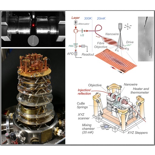
Nano-Optomechanical Force Sensor at mK Temperatures
Since the invention of the atomic force microscope (AFM), mechanical force sensors have been among the most sensitive probes in scanning microscopy. In an effort to further push the limits of probe temperature and sensitivity, researchers from the Néel Institute (Grenoble, France) have now cooled down a nanowire-based force sensor to 32 mK.
Based on an all-optical single-photon detection method and attocube nanopositioners (ANPxyz101/ANSxyz100), the nanowire was kept in focus during cooldown, and subsequently characterized. At mK temperatures, the group demonstrated record sensitivities for scanning force probes, which enable vectorial imaging of weak forces, such as the interaction of a spin qubit with a nanoresonator.
This measurement was realized with the ANPz101/LT - linear z-nanopositioner.
Further reading:
F. Fogliano et al., Nat. Commun. 12, 4124 (2021)
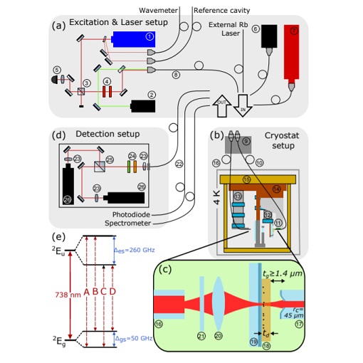
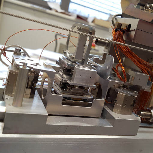
Fiber-Based Microcavity with inserted Diamond Membrane at 4 K
For the fields of quantum sensing, quantum communication, and quantum memories stable solid-state emitters (e.g. color centers) are from highest interest. M. Salz et al. investigated fiber-based microcavities coupled to in single crystal diamond (SCD) membrane incorporated silicon vacancy centers (SiV-). Within the experimental setup and with the help of several attocube nanopositioners a Purcell enhancement of the excited-state decay into the cavity mode was examined at 4K.
The experimental setup consists of different subparts like: excitation & laser setup, detection setup, and the cryostat setup (b, c) - within the positioners are used. The multimode fiber (16) is mounted on a 3D ANPx101-ANPx101-ANPz102-stack (13), the dielectric mirror (19) is mounted on a further 3D-stack consisting of two ANPx311 and one ANPz51 (12). Due to the used piezo-driven nanopositioners an exact movement of the mirror to the cavity fiber during the experiment can be ensured, moreover, the mirror can be moved away from the fiber during cooldown to avoid an unwanted crashing of both parts.
This measurement was realized with the ANPx101/LT - linear x-nanopositioner, the ANPz51/LT - linear z-nanopositioner, the ANPx311/LT - linear x-nanopositioner, and the ANPz102/LT - linear z-nanopositioner.
Further reading:
M. Salz et al., Appl. Phys. B. 126.8, 1-13 (2020)
Electro-Optic Converter at mK
Prof. Dr. J.M. Fink and his research group brought us one step closer to seminal technologies like quantum secure communication, modular quantum computing clusters, and powerful quantum sensing networks. In a recent experiment "Bidirectional Electro-Optic Wavelength Conversion in the Quantum Ground State" has been examined with the help of radiative cooling and a triply resonant ultra-low-loss transducer operating at millikelvin temperatures.
With the used setup the problem of the high sensitivity of quantum states encoded in microwave frequency excitations to electronic or thermal noise could be tackled. Two GRadient INdex (GRIN) lenses are used to focus input and output beams (red), each lens is attached to one xyz-piezo positioning stack from attocube. Moreover, the prism (light blue) is moved horizontally and the microwave tuning cylinder (gold) vertically with two additional attocube positioners. In total, eight stages are used to perfectly adjust and align the different positions of the system to each other - and that at a base temperature of below 10 mK.
This measurement was realized with the ANPx101/LT - linear x-nanopositioner, and the ANPz101/LT - linear z-nanopositioner.
Further reading:
W. Hease et. al., PRX Quantum 1.2, 020315 (2020)
G-Factor Anistropy Examined in High Magnetic Fields & at 200 mK
In a collaboration of the Zumbuhl Group with RIKEN, SAS and UCSB an experiment for showing the separation of the isotropic and anisotropic g-factor corrections in GaAs quantum dots has been performed. To erperimentally determine the g-factor corrections, the spin splitting was extracted by measuring the tunnel rates for an in-plane magnetic field with various strengths and directions. Here they measure and separate the isotropic and anisotropic corrections to the g-factor in two GaAs devices, finding good agreement with recent theory.
This was done with the help of attocube's rotator ANRv51/RES on which the sample was mounted on and precisely rotated in the plane of a magnetic field. This experiment was performed in a dilution refrigerator at a temperature of 200 mK and magnetic fields up to 14 T. Such high fields, applied in an arbitrary in-plane direction, are only accessible with a sample rotator since vector magnets are limited to a few Tesla.
This measurement was realized with the ANRv51/RES/LT/HV - rotator (360° endless).
Further reading:
L. C. Camenzind et al.; Phys. Rev. Lett. 127, 057701 (2021)
Spin relaxation record at 25 mK and 14 T
Spin qubits based on quantum dots are promising candidates as building blocks for future quantum computers. In 2018, an international collaboration (Basel, Saitama, Tokyo, Bratislava and Santa Barbara) successfully demonstrated a new mechanism for electron spin relaxation for the first time experimentally, 15 years after this phenomena has theoretically been predicted. Working at 25 mK DR and in up to 14 T, a new record of electron spin lifetime of over a minute in a semiconductor nanostructure - GaAs - was achieved at around 0.6 T.
For this setup attocube's encoded ANRv51 was used as it perfectly fits the requirements of a mK temperatures and high magnetic fields system. Moreover, the sample of a single-electron quantum dot formed in a GaAs 2D electron gas could perfectly be aligned arbitrarily to the in-plane magnetic field with respect to the crystal axis.
This measurement was realized with the ANRv51/RES/LT/HV - rotator (360° endless).
Further reading:
L.C. Camenzind et al.; Nat Commun 9, 3454 (2018)
3D micro-structure sample positioning in 4 dimensions in a µ-RHEED/SEM system
Sohei Nakatsuka et. al from Tohoku University and Osaka University, Japan have designed a system for analysing a 3D micro-shaped structure on a Si substrate. Their system combines a micro-beam reflection high-energy electron diffraction (µ-RHEED) and scanning electron microscopy (SEM). Sample Manipulation is done in four dimensions via a mechanical rotation stage for glancing angle (Θ) and a 3D nanopositioner stack mounted onto the mechanical device. The 3D stack consists of two attocube ECSx3030 for xy-movement and one ECR3030 for azimuth angle (Φ) rotation. The sample manipulator enables precise positioning and rotation of the 3D microstructured sample to identify surface structures like surface morphology, surface orientation defined by Miller index, surface ordering, and surface reconstructed structures. attocube EC* series stages are the perfect fit due to highest precision within extrem environments like ultra-high vacuum and harsh radiation.
This measurement was realized with the ECSx3030/StSt/NUM+/HV.
Further reading:
e-J. Surf. Sci. Nanotechnol. 19, 13-19 (2021)
Fiber alignment at mK conditions
The step from theoretical to practical quantum computing requires not only components for quantum entanglement but also a low-loss and robust network for further data distribution. The interface between superconducting processors and optical telecom networks is one of the open questions in the quantum community. A possible solution was now presented by the group of Johannes Fink from the Institute of Science and Technology Austria (Klosterneuburg, Austria). Their bidirectional and chip-scalable converter opens a way to integrate superconducting circuits into large scale optical fiber networks using a nanomechanical transducer. The precise alignment and stable connection of the optical fibre to the microwave chip at 10 mK temperatures required a stiff set of ANP101 positioners for x,y, and z movement. This new device allows using pump-powers orders of magnitudes lower than previously reported transducers which reduces optical heating and conversion noise that currently still hinders a quantum limited operation.
This measurement was realized with the ANPx101/RES/LT - linear x-nanopositioner, the ANPz101/RES/LT - linear z-nanopositioner, the ANPx101/ULT/RES+/HV - Linear x-Nanopositioner, and the ANPz102/ULT/RES+/HV - linear z-nanopositioner.
Fiber Array Alignment with Multi-Axis Piezo Stages
For optical data transmission fibers need to be precisely attached to different components. A wide variety of components is used for optical, photonic and electronic modules, simultaneously their complexity increases. Therefore, it is inevitably necessary to have suitable and reliable products to be one of the leading providers in the field of micro assembling. The fundament for the assembly of photonic devices is particularly precision of multi-axis movements.
Due to the fact that the ECS series stages can be driven in coarse and fine positioning mode the fiber can easily be moved on a mm level to the desired position and then be adjusted on a nm level with highest precision. Piezo driven stages also captivate with long term stability when a specific position needs to be held over an extended time period. The modular design enables multi-axis solutions by simply combining different positioners and types of movements.
This measurement was realized with the ECSx5050/Al/NUM/RT, the ECGt5050/Al/NUM/RT, and the ECR5050hs/Al/RT.
Combined Laser Beam Epitaxy and Low-Temperature STM using ANPx321 Positioners
Adding new functionalities to an STM is a demanding task due to the strict requirements to the operating condition. On the other hand, being able to deposit material while using an STM enables to synthesize new material or characterize it more efficiently, because it frees from the need to interact with the sample.
The group of Prof. Qing Huan (Chinese Academy of Science, Beijing) has achieved such a feat by combining laser molecular beam epitaxy and a cryogenic STM. The STM operates at 5 K in ultra-high vacuum conditions and offers a sample-moving range of 15 x 15 mm2. The integrated ANPx321 positioners (closed-loop configuration) feature a positioning accuracy better than 1 µm. The multi-use STM demonstrates its performance by growing and analyzing various materials. Overall, the group expects to have provided a platform suitable for systematic research on new materials, including superconductors.
This measurement was realized with the ANPx321/LT/HV - linear x-nanopositioner.
Further reading:
He, Ge, et al., Rev. Sci. Instrum., 91 (1), 013904 (2020)
ANR31 Rotator used at 350 mK & 35 T
High precision in extreme conditions was a major requirement for a collaboration led by Nicholas Butch at the NIST and the University of Maryland (USA). While working at magnetic fields up to 65 T, they observed an exotic “re-entrance” effect of superconductivity in UTe2. As superconductivity and magnetic fields are usually not coexistent, their findings highlight a new kind of explanation for superconductivity.
For the magnetoresistance measurements of up to 35 T in Tallahassee, an ANR31 rotator aligned the sample’s axis precisely with respect to the applied DC field. As the superconductive phase is stable only over a narrow angular range at high fields, precision was a major prerequisite.
This measurement was realized with the ANR31/LT/HV rotator made from Titanium and CuBe.
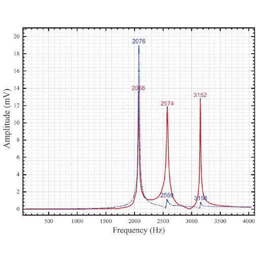
Resonance Frequency of an ANSxy50 made of titanium
attocube scanners, especially the ones made for cryogenic and magnetic environments are often implemented in highly sensitive scanning probe microscopes. One of the major issues in such setups is stability and vibrational stiffness. For such an application, the group of Bert Voigtländer from the institute of Quantum Nanoscience at Forschungszentrum Jülich (Jülich, Germany) detected the resonance frequencies of a standard ANSxy50 positioner made of titanium. The top plate of the scanner was removed for their purpose and the device was fixed on a support. The scanner body was excited with an external piezoelectric element while the response voltage (due to the piezoelectric effect) of the integrated piezo elements detected the resulting vibrations of the scanner. The measurements showed clear resonance peaks at frequencies in the kHz regime, namely 2.1 kHz (1st mode), 2.6 kHz (2nd mode) and 3.2 kHz (3rd mode), showing the high stability of this attocube scanner. Comparing the results with simulations of the resonances idetified these with complex modes with dominant vibrating directions in z (1st mode), and in perpendicular modes in the x-y plane (2nd and 3rd mode). After this successful evaluation, the Jülich group will use these scanners, which combine high stiffness with a large scan range, in a low temperature four-tip scanning probe microscope.
This measurement was realized with the ANSxy50/LT xy-Scanner made from Titanium.
Near-Field Scanning Microwave Microscope at 30mK
Scanning techniques such as atomic force microscopy (AFM) or scanning tunnelling microscopy (STM) offer a wide range of material investigation possibilities. Depending on the environmental conditions and the required scanning resolution scanning probe microscopes are hard to design and setup and not seldom homemade devices, adapted to their special proposes and requirements. A new low temperature near-field scanning microwave microscope working at 30 mK, designed to meet emerging needs of the quantum technologies sector, was now developed by the group of Sebastian de Graaf at NPL (National Physical Laboratory, Teddington, UK) in collaboration with the group of Prof. Sergey Kubatkin (Chalmers University of Technology, SE). It combines microwave characterization up to 6 GHz with STM or AFM techniques. The environment of a dilution cryostat makes special demands on the stability and stiffness of the used components. The group used a set of ANPx100 and ANPz100 nanopositioners (former versions of the ANP101 positioners) to align the sample with the tip in x, y, and z direction and a small ANPz51 positioner for the RF waveguide positioning. First verifications of the instrument showed the capability to image dielectric contrast down to the single microwave photon regime.
This measurement was realized with the ANPx101/LT/HV - linear x-nanopositioner, the ANPz101/LT/HV - linear z-nanopositioner, and the ANPz51/LT/HV - linear z-nanopositioner.
Further reading:
S. Geaney et al; Scientific Report 9, 12539 (2019)
A quantum network node and register based on silicon-vacancies in diamond
The realization of a quantum network node is a fundamental requirement for a later quantum network or even quantum internet. Such a quantum register receives or emits information without disturbing the underlying quantum state. Now, the groups of Marko Loncar and Mikhail Lukin at the Havard University (Cambridge, MA, USA) present an elementary quantum network node based on a silicon vacancy color center inside a diamond nanocavity. This optically active point defect in the diamond lattice is characterized by a self-made mK confocal microscope based on cryogenic nanopositioners and a cryogenic apochromatic objective from attocube inside a dilution cryostat. Additionally, the authors demonstrate the working principle of the node as quantum register by coupling the system to incoming optical photons, as well as a nearby nuclear spin featuring a 100ms long decoherence time. Their work marks a first step towards the realization of a first-generation quantum repeater.
This measurement was realized with the ANPx101/LT - linear x-nanopositioner, and the ANPz102/LT - linear z-nanopositioner.
Further reading:
C.T. Nguyen et al, Phys. Rev. B 100, 165428 (2019)
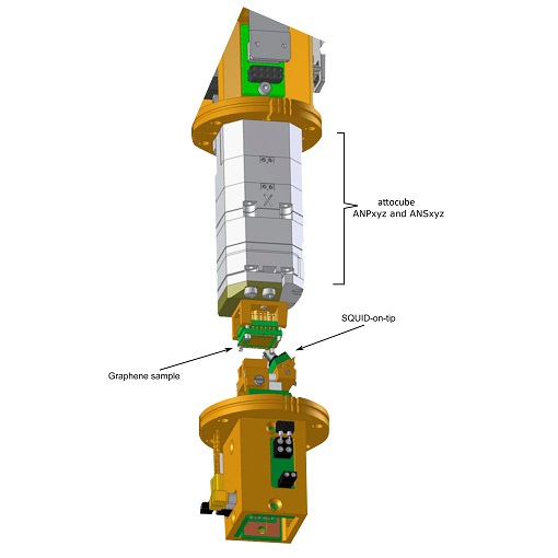
Light-matter coupling in TMD monolayers and heterostructures
Scanning optical micro-cavities have been used by two collaborating groups to study light-matter coupling phenomena in semiconductor transition metal dichalcogenide (TMD) monolayers and heterostructures. The groups of David Hunger (Karlsruher Institut für Technologie, Karlsruhe, Germany) and Alexander Högele (Ludwig-Maximillians-Universität München, Germany) explored atomically thin TMD semiconductors with scanning-cavity hyperspectral imaging at room and cryogenic temperatures. To this end, WSe2 monolayer and MoSe2-WSe2 heterobilayer were coupled to a tuneable cavity consisting of a fiber-based micro-mirror at one end and a planar micro-mirror with the sample at the other end, as sketched in figure 1. For room-temperature monolayers in strong-coupling, spatial maps of new half-matter and half-light quasiparticles – so-called exciton polaritons – were correlated to maps of exciton extinctions and fluorescence [1]. Heterobilayers were explored in the weak-coupling regime at 4 K to demonstrate Purcell enhancement of layer-indirect excitons and to determine their oscillator strength [2]. To ensure the required stability, the experiments employed an ECSx3030 and ANPx101 positioner for ambient and cryogenic conditions respectively, to realize the tuneable cavity and align the fiber with respect to the sample
This measurement was realized with the ANPx101/LT - linear x-nanopositioner, the ECSx3030/Al/RT, and the ANPz102/LT - linear z-nanopositioner.
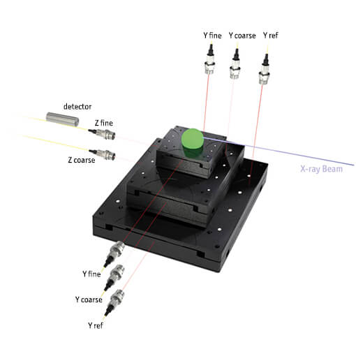
Piezo-based Positioning for Magnetic Field Detection
X-rays, also referred as synchrotron radiation, serve as an important tool to observe the structure and dynamics of matter. The radiation is generated by bending magnets, wigglers or undulators. While bending magnet and wiggler radiation have a broader spectrum of photon energies, undulator generates narrow peaks, i.e. bright and coherent radiation at specific harmonics. This specific peak spectrum and defined photon energy is the main advantage of undulator radiation. Dr Carsten Kuhn and his group at the Helmholz-Zentrum in Berlin (Berlin, Germany) developed the new generation of undulators for the storage ring BESSY II. In order to optimize the resulting photon energy, the magnetic properties of cryogenic undulators need to be characterized precisely at different temperatures by movable Hall probes. Therefore, they designed a measurement slide with six attocube positioners to align the hall probe with respect to the undulators' magnets. With this precise analysing setup, the position accuracy of the Hall-probes is at least 5 μm and 20 μrad.
This measurement was realized with the ECSx3030/StSt/NUM/HV, and the ECSx3030/StSt/NUM/HV.
Life Science: 3D Imaging System Showing Natural Colour
Interesting features in life science and biology often span several orders of magnitude in size. A complete optical study requires to resolve structures from sub-micrometer to centimeter, thus high resolution is a fundamental need. In addition, fast acquisition times are demand, as any movement during the image-taking process will cause blurr.
The group of Prof. Ming Lei at the State Key Laboratory of Transient Optics and Photonics (Xi'an Institute of Optics and Precision Mechanics, Chinese Academy of Sciences, Xi’an, China) developed such a 3D microscope with a lateral resolution of 580 nm.
The possibility to obtain full colour 3D images and 3D morphological data in the size range of typical insects opens the door for many different types of entomological investigations. Three attocube ECS positioners actuate a microscopic stage to move and align the sample in all three dimensions. The positioners are perfectly suited for such an application as they provide a travel range of at least 20 mm with a typical step size of less than 100 nm.
This measurement was realized with the ECSx3030/Al/NUM/RT.
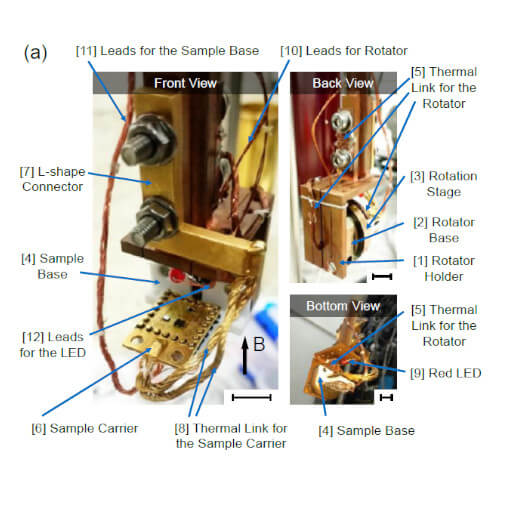
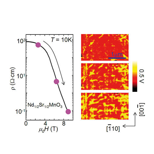
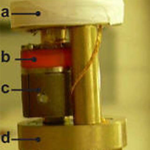
Rotating transport measurement setup at 25mK
When designing a setup for mK applications material choice and thermalization is crucial. Titanium becomes superconducting at temperatures below 400 mK consequently, the thermal contact to the sample is not ensure anymore. At Peking University (Beijing, China), Dr. Pengjie Wang from Xi Lin group has chosen the beryllium-copper version of the ANR101 positioner with resistive readout to realize their low-electron-temperature sample rotation system for transport measurements inside a dilution cryostat. The rotator allows to orient the sample in-situ with respect to a high magnetic field of up to 10 T.
The dilution cryostat with a diameter of 81 mm offers the required space for the rotator setup, see picture. The sample holder is designed for the use of up to four sample, each 5 mm x 5 mm large, a red LED is installed to illuminate the samples at 4 K for an easier orientation. The measured electron temperature in the setup is 25 mK, the same as the environmental temperature.The setup is designed for transport measurements and material characterization at ultra-low electron temperatures. A first application shows the tilt-induced localization and delocalization of the second Landau level of the two-dimensional electron gas - an experiment for which a pressurized liquid ³He cell had been necessary elsewise.
(Figure reproduced from Rev. Sci. Instrum. 90, 023905 (2019); doi: 10.1063/1.5083994, with the permission of AIP Publishing)
This measurement was realized with the ANR101/RES/LT - rotator (360° endless).
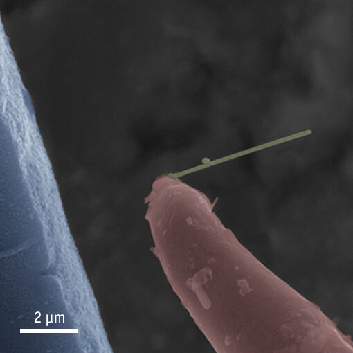
Micromechanical Testing of Silver Nanowires
The small size of specimens often imposes significant challenges for preparation and testing. To overcome these difficulties, Prof. Horacio Espinosa’s group at the Mechanical Engineering Department in Northwestern University, USA, has developed a microelectromechanical system that allows mechanical testing of nanowires (see left figure). The system is capable of simultaneous four-point electrical measurements, therefore enabling piezoresistivity and -electricity measurements.
In order to mount the silver nanowires, they employed an attocube nanomanipulator, composed of three stacked ECS3030 positioners, one for each axis of movement. The nanomanipulator is positioned inside an SEM chamber and interfaced to the ECC100 piezo-controller outside the chamber.
This measurement was realized with the ECSx3030/Al/RT.
Further reading:
R.A. Bernal, et al., Small 10, 725 (2014)
Sample positioning in scanning transmission x-ray microscope at SLAC
We use attocube linear stages with optical and resistive encoders for positioning of samples relative to high resolution x-ray optics in a scanning transmission x-ray microscope. The picture shows a magnetic excitation called “soliton” that is the result of a spin polarized current injected into a thin ferromagnetic Co/Pt multilayer. The injected spin causes a localized oscillation of the magnetization at the spot where the current is injected, here a nano contact with a 150 nm diameter in the center of the picture. Time resolved scanning transmission x-ray microscopy using magnetic circular dichroism as a contrast mechanism is used to obtain an image of the magnetic soliton.
(Dr. Hendrik Ohldag, Stanford Synchrotron Radiation Laboratory, SLAC National Accelerator Laboratory.)
This measurement was realized with the ANPx101/UHV - linear x-nanopositioner, and the ANPz102/UHV - linear z-nanopositioner.
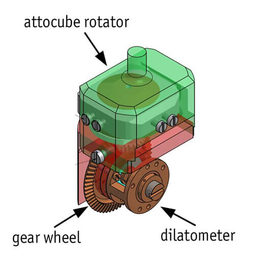
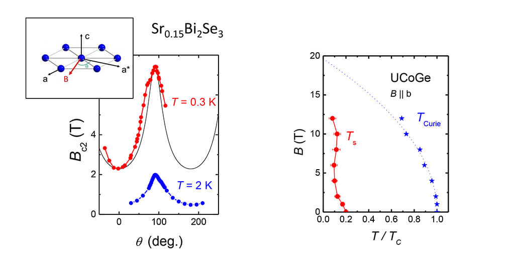
Angle-dependent characterizations of materials at mK temperatures
attocube's rotators offer a way to use the full magnetic field of a 1D magnet for field-angle dependent transport measurements at the sample. This benefit is used by the group of Anne de Visser at the Van der Waals - Zeeman Institute (University of Amsterdam, NL) in two setups with an ANR51 and an ANRv220 both in a closed loop configuration.
Magnetotransport measurements as a function of the angle θ in the trigonal basal plane of the topological superconductor SrxBi2Se3 revealed a large two-fold anisotropy of the upper critical field Bc2. Such a rotational symmetry breaking of Bc2(θ) cannot be explained with standard models, and indicates unconventional superconductivity with an exotic order parameter. More about this work can be found at [1].
In the second setup a home-built compact dilatometer was mounted on the ANRv220 in a dilution refrigerator. This was used to measure the anisotropy in the ferromagnetic and superconducting phase diagram of a single crystal of UCoGe by applying magnetic fields up to 14 T along the different crystallographic axes [2].
This measurement was realized with the ANR51/RES/LT - rotator (360° endless), and the ANRv220/RES/LT - rotator (360° endless).
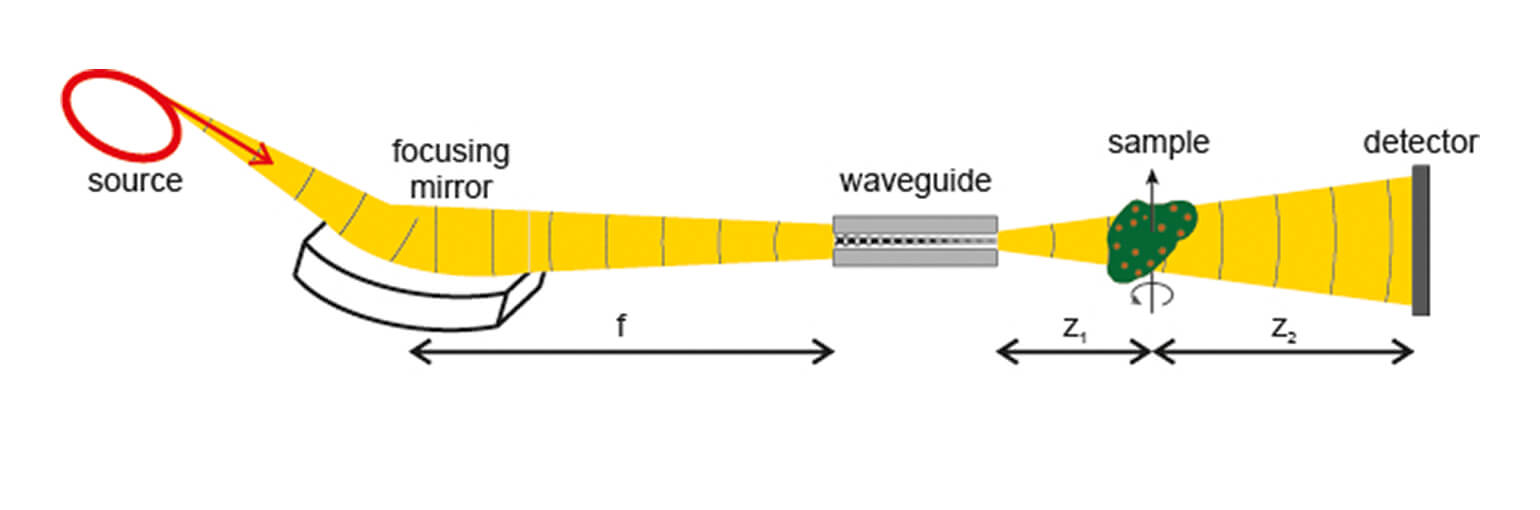
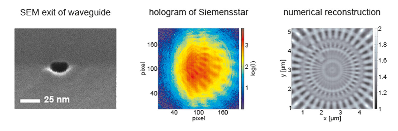
Lensless Imaging with X-Ray Waveguides
A synchrotron generated X-Ray beam was coupled into an X-Ray waveguide located in the focus of Kirkpatrick-Baez mirrors. The resulting filtered wave was then used to illuminate a sample coherently, yielding a magnified hologram of the sample recorded by a pixel detector. Several linear positioners, goniometers, and rotators were applied for precision alignment of the waveguide with respect to the sample, which in turn was mounted on a high-precision tomographic rotation stage.
This measurement was realized with the ANPx101/UHV - linear x-nanopositioner.
Further reading:
S. Kalbfleisch et al., AIP. Conf. Proc., 1234, 433-436 (2010)
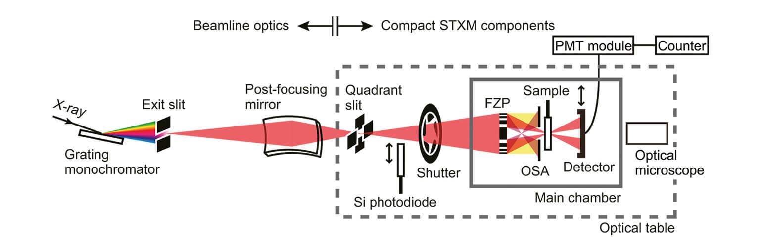
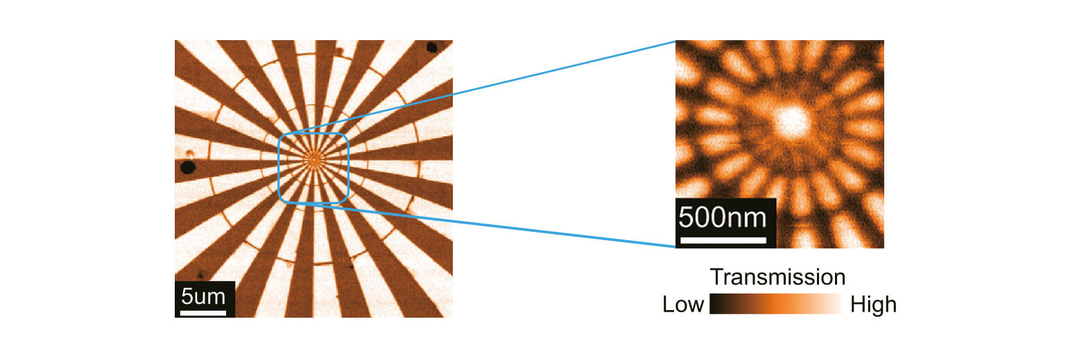
New Stable and Portable X-Ray Microspectroscope at KEK
At the high energy research accelerator KEK in Japan, Dr. Takeichi et al. designed a novel X-Ray microspectroscope for high resolution composition analysis. The setup is comprised of 11 attocube ECS stepping positioners and a dedicated scanner for sample imaging. All the positioners are equipped with optoelectronic sensors and can be digitally controlled. The sample stage is stabilized via attocube’s interferometric FPS3010 sensor with a resolution of 25 pm. The whole four-stack-setup is compact enough to fit into a vacuum chamber of only 220×310×200 mm3. First measurements show the resolution of the new instrument to be approximately 40 nm.
This measurement was realized with the ECSx3030/StSt/HV, and the .
Further reading:
Y. Takeichi, et al, Rev.Sci.Instr. 87, 013704 (2016)
Detecting vibration propagation and parasitic motions with picometer resolution
Exact sample positioning in synchrotron beamlines requires position detection with highest resolution. A group at the Diamond Light Source designed a sample positioning system with three positioners for x, y, z movements. To determine the error motions, eight axes of three IDS3010 devices were triggered for synchronous data acquisition, controlling the movement with BiSS-C interface. They identified parasitic motions of only 100 pm that were caused in the non orthogonal fixing of the positioners. These smallest amount of deviation can be detected in Ultra-high vacuum only - and with the IDS3010.
(Trevor Bates, Brian Nutter, Diamond Light Source Limited, Oxfordshire, England)
This measurement was realized with the ECSx5050/Al/RT, and the Displacement Measuring Interferometer.
Outgassing Behaviour in Ultra-High Vacuum
Experiments in Ultra High Vacuum (UHV) conditions require highest precision and care in manufacturing of the respective equipment. The outgassing behavior is a crucial factor when researchers decide for new instruments in their setups. This application note describes measurements of the outgassing data of an attocube rotator with an integrated resistive encoder ANR101/ RES/UHV.
(The tests were carried out at the BESSY synchrotron facility in Berlin, Germany.)
This measurement was realized with the ANR101/RES/UHV - rotator (360° endless).
The Axion Dark Matter eXperiment - Nano Precision in Extreme Conditions
The Axion Dark Matter eXperiment (ADMX) seeks to prove the existence of the axion and reveal the composition of dark matter by looking for the resonant conversion of dark-matter axions to microwave photons in a strong magnetic field. The new high-frequency Sidecar experiment, developed by Christian Boutan at the University of Washington (now at the Pacific Northwest National Laboratory) is a miniature axion haloscope that fits inside of the ADMX insert and has the capability of searching for axion masses between 16µeV - 30µeV. Two positioners are required for the essential functions of tuning the cavity and adjusting the antenna coupling at mK temperatures in a 8 Tesla field. attocube's ANR240/RES and ANPz101eXT12/RES were employed in this pathfinder experiment.
This measurement was realized with the ANR240/RES/LT - rotator (360° endless), and the ANPz101eXT12/RES/LT - linear z-nanopositioner.
Transition from slow Abrikosov to fast moving Josephson vortices
attocube proudly presents his cutting edge application using the ANR31 rotator: They observed the formation of fast moving Josephson vortices, which depends critically on the angular alignment. Using the ANR31, they were able to rotate the sample below 2 K with better than 0.1° precision and could observe no drifts while sweeping temperature and magnetic field.
This measurement was realized with the ANR31/LT rotator made from Titanium and CuBe.
Angle-dependent transport measurements at 40 mK
Based on an attocube systems rotator ANR30/LT a rotation stage for angle-dependent transport measurements in magnetic fields up to 33 T and temperatures down to 40 mK was built at the user facility of the High Field Magnet Laboratory in Nijmegen.
The mixing chamber of the commercially available dilution refrigerator from Leiden Cryogenics offers only a limited space of 17 mm in diameter. Hence, the ultra compact attocube rotator ANR30/LT is the positioner of choice for this task. The rotator is fixed on a plastic (Hysol) dilution refrigerator insert.
This measurement was realized with the ANR31/LT rotator made from Titanium and CuBe.
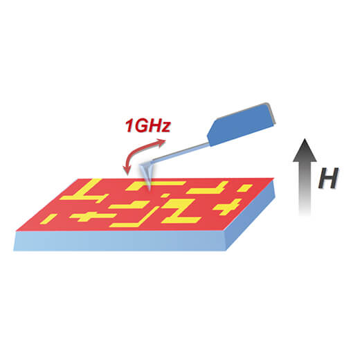
Scanning Microwave Impedance Microscopy at 4 K and 9 T
A set of linear positioners and scanners made for cryogenic application was implemented into a microwave impedance microscope located inside a liquid Helium flow cryostat equipped with a 9 T superconducting magnet. The 1 GHz microwave signal was guided to the cantilever probe, which detected the dielectric constant and conductivity contrast of the sample during scanning. The system is a versatile tool for fundamental research on complex materials and phase transitions under various conditions.
This measurement was realized with the ANPx101/LT - linear x-nanopositioner, and the ANPz102/LT - linear z-nanopositioner.
Performance Test of the ANPz30/LT at 35 mK and 15 Tesla
The precise performance of nanopositioning elements is of great importance in order to realize instrumental setups which work reliably under extreme environmental conditions. Although attocube systems’ positioners have been tested at low temperatures down to 10 mK and at high magnetic fields up to 28 Tesla, their successful performance has never been demonstrated when both environmental conditions were simultaneously applied. A real challenge, furthermore, is to carry out such a test in a 3He/4He environment due to the fact that 3He carries a magnetic spin which becomes polarized in magnetic fields. This influence on the positioner’s operation was investigated for the first time in this application.
This measurement was realized with the ANPz30/LT - linear z-nanopositioner.
Magnetic Resonance Imaging of Nanoscale Virus at 300 mK
attocube’s ANPx51 positioners were used in an MRFM setup with the task to precisely and reliably position a magnetic tip and a copper nanowire to close proximity of an ultra-sensitive cantilever. The MRFM setup was applied to investigate and reconstruct the 1H spin distribution of Tobacco Mosaic Virus particles, representing a 100-million fold improvement in volume resolution over conventional MRI.
This measurement was realized with the ANPx51/LT - linear x-nanopositioner.
Photoluminescence measurements in fields up to 28 T
The attocube systems positioners ANPxyz100/LT have been used in a setup for optical measurements in liquid 4He temperature and magnetic fields up to 28 T at the Grenoble High Magnetic Field Laboratory. In the setup laser excitation is delivered using a single-mode fiber and is focused onto the sample with two microlenses. A multimode fiber is used for photoluminescence (PL) collection.
This measurement was realized with the ANPx101/LT - linear x-nanopositioner, and the ANPz102/RES/LT - linear z-nanopositioner.
Scanning Hall Probe Microscopy at 300 mK with ANP positioners
The magnetic properties of superconducting and ferromagnetic materials at ultra-low temperatures represent some of the most interesting contemporary problems in condensed matter physics. These properties are typically investigated using a magnetic force microscope or a scanning Hall probe microscope (SHPM). In this note, we report on a self-built SHPM capable of working at temperatures as low as 300 mK and magnetic fields of up to 10 T, while still having sub-micron lateral spatial resolution.
This measurement was realized with the ANPx101/LT - linear x-nanopositioner, and the ANPz102/RES/LT - linear z-nanopositioner.
mK STM Image with Atomic Resolution
STM image of an aluminum (100) surface with atomic resolution. The image size is about 29 x 20 nm2. The corrugation is between 300 fm and 800 fm, depending on the direction of the line profile. Defects show up as ring-like structures with different radii depending of their depth. The image was measured in a homebuilt mK-STM at the Max-Planck Institute for Solid State Research in Stuttgart, which uses a cryogenic attocube ANPz51 positioner for coarse approach.
(Image courtesy of Department of K. Kern, Max-Planck Institute for Solid State Research, Stuttgart, Germany)
This measurement was realized with the ANPz51/LT - linear z-nanopositioner.
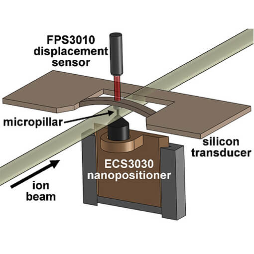
Measurements of Irradiation-Induced Creep
S. Özerinç and his colleagues at the University of Illinois at Urbana-Champaign have developed an apparatus for measuring irradiation induced damage and stress on the nanometer scale. Using attocube's ECS3030 as well as the FPS3010 interferometer, the system can measure in situ the deformation of mechanically stressed micro-pillars, during which the pillars are irradiated with heavy MeV ions. The apparatus provides a new and effective approach to accelerate the evaluation of promising materials for future nuclear power plant applications.
This measurement was realized with the ANPx101/RT - linear x-nanopositioner, and the Displacement Measuring Interferometer.
Mapping and Manipulation of Leakage Currents in a Nanostructure
In this application note, attocube’s smallest titanium positioners (ANPx51/RES and ANPz51/RES) are used as part of an atomic force microscope (AFM) inside a Janis ³He cryostat with a base temperature of 280 mK. The setup is a combined low temperature AFM and scanning tunneling microscope (STM), which is emploied to carry out scanning gate microscopy experiments on various nanostructures. In these measurements the positioners are used to move the metallic tip directly above the nanostructure predominantly at 4.2 K but also as low as 280 mK.
This measurement was realized with the ANPx101/RES/LT - linear x-nanopositioner, and the ANPz102/RES/LT - linear z-nanopositioner.
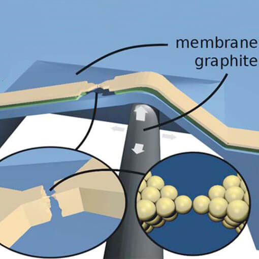
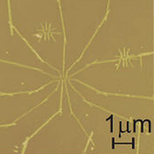
Mechanically Controlled Multi-Contact Break Junctions
In this application, small tips made from either glass or graphite were used to locally deform a silicon membrane, creating break junctions in a very controlled fashion. The tips with a typical radius between 50 and 200 microns were precisely controlled using attocube’s nanopositioning technology. The approach of locally creating and controlling individual break junctions can be used to study the influence of optical excitations on the conductance of individual molecules and for controllable metallic single-electron transistors.
This measurement was realized with the ANPx51/LT - linear x-nanopositioner.
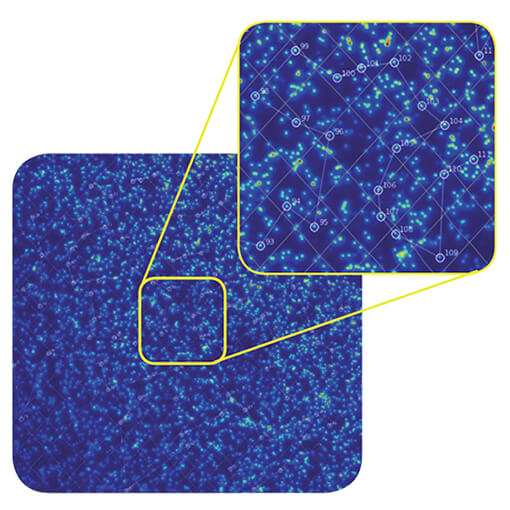
Automatic Mapping of Semiconductor QDs
Returning to interesting sample positions has never been easier: Yves Delley from the Quantum Photonics Group (QPG) at the ETH Zurich have - based on attocube positioners with resistive encoders made for cryogenics - built a micro-photoluminescence (PL) setup and automated it to a great extent. They programmed a fully automated routine for raster-imaging a full sample of up to 4 x 4 mm2 as well as implemented an auto-focus routine. Once initiated, the positioners are moved frame-by-frame and a CCD camera takes images of the PL of their semiconductor quantum dot samples. Knowing the coordinates of all individual images, it is easy to put together a complete map of the sample (see figure ).
“Now, we have to select the interesting dots, at which we want to take a closer look”, says Yves Delley, the responsible project researcher at QPG and gags: “Yet, in order to find the shortest route between all these quantum dots, we would need a quantum computer to solve this problem.”
(Image kindly provided by Yves Delley, Quantum Photonics Group, ETH Zurich, Switzerland)
This measurement was realized with the ANPx101/RES/LT - linear x-nanopositioner, and the ANPz102/RES/LT - linear z-nanopositioner.
3D g-Factor Mapping of Single Quantum Dots
A xyz linear positioning stack combined with a rotator was used in a novel fiber-based confocal microscope, dedicated for the investigation of certain nanostructures such as InGaAs quantum dots (QDs) using magneto-photoluminescence (PL). The specific arrangement of positioners enabled scientists in this experiment to tilt and rotate samples at low temperature with respect to a magnetic field of up to 10 T while maintaining focus on a single QD.
This measurement was realized with the ANPx101/LT - linear x-nanopositioner, the ANPz101/LT - linear z-nanopositioner, and the ANR101/LT - rotator (360° endless).
Sample Nanomanipulation of 1-D Nanostructures
The group of Horacio Espinosa at Northwestern University has employed attocube‘s ECS3030 positioners (controlled by an ECC100 piezo-controller) to accomplish nanometer precise manipulation of various nanotubes inside a SEM chamber. Once a nanowire is picked up, the manipulator is used to position it on top of a MEMS device for testing elastic strength as well as for four-point electrical measurements.
This measurement was realized with the ECSx3030/StSt/HV.
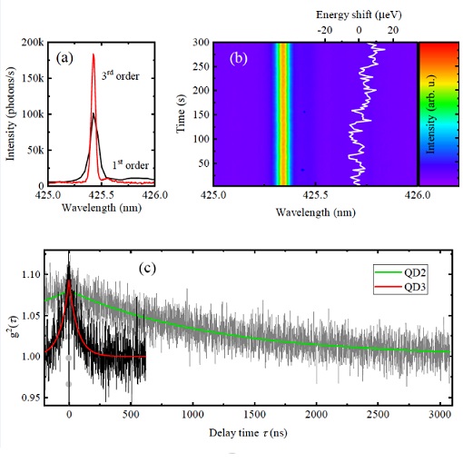
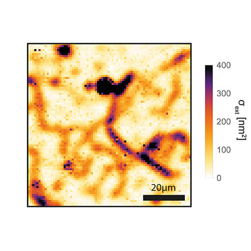
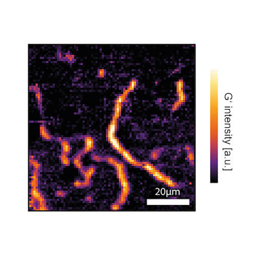
Cavity Enhanced Raman Microscopy
level signals remain intrinsically small. Recently Th. Hümmer et al from the group of Prof. Hänsch achieved a more than sixfold amplification by putting the sample inside a tiny cavity. The cavity formed by the sample and a micro mirror on the tip of an optical fiber (1) can be scanned by a set of attocube’s ECSx3030 positioners to obtain images with close to optical resolution. The micro cavity is adjusted with some tens of pm resolution using another ECS positioner and an additional piezo. The signal is enhanced due to the Purcell effect stemming from the enhanced photon lifetime in a small cavity volume (2).
The group around Dr. Hunger at the LMU Munich applied the new method to some carbon nanotubes leading to clear pictures showing (3) the extinction cross-section and (4) the Raman signal of the G’ mode. “The cavity amplifies both the Raman scattering process as well as absorption from the sample. This allows one to combine ultrasensitive absorption microscopy with Raman imaging within a single measurement.”, explains Dr. Hunger. The group is confident to improve the method further boosting the signal enhancement by several orders of magnitude in the future.
(*Pictures are under Creative Commons Attribution 4.0 international license)
This measurement was realized with the ECSx3030/StSt/HV.
Enabling Haptic Assembly of Micrometer Structures
M. A. Srinivasan of MIT, USA and UCL, London, with support from TUM-IAS, Munich, has developed a micromanipulator with an haptic interface to enable manual exploration, manipulation, and assembly of micro-structures. In collaboration with A. Schmid of UCL, London, S. Thalhammer of Helmholtz Zentrum, Munich, and R. Yechangunja of Yantric, Inc., USA, he has demonstrated manual grasping and moving of 10 to 100 µm sized objects with direct haptic feedback of the gripping force in real-time, so that the objects can be placed in three dimensions with nanometer precision.
A force-sensing microgripper with 100 µm opening is mounted on an ANPxyz101/NUM stack of attocube’s closed loop positioners. Measured forces by the microgripper in the micro-Newton range are scaled up and exerted on the operator’s fingers through a haptic interface.
This measurement was realized with the ANPx101/RT - linear x-nanopositioner, and the ECSx3030/Al/NUM/RT.
Tuning of a Fabry-Pérot Resonator for High Field
P. Neugebauer and his team have integrated attocube's ANPz51 in a new cavity design to measure high-frequency electron paramagnetic resonances (HF-EPR).
Among other advantages, the group was able to move a mirror in-situ within the resonator, to find the right mode and precisely fine-tune its position.
This measurement was realized with the ANPz51/RT - linear z-nanopositioner.
Controlling Ultra-Fast Electron Emission
The dynamics of electrons emitted from a sharp tungsten tip triggered by femtosecond laser pulses have been investigated. The setup shown to the left is situated in an UHV chamber at p = E-10 mbar pressure. A xyz positioning stack enables precision alignment of the tip. Photoelectron spectra are recorded while the phase between carrier wave and intensity envelope is varied in small steps. The lower figure shows two electron spectra, recorded with a phase difference of 180°. In a), pronounced peaks are visible caused by interference of two electron wave packets emitted during subsequent optical cycles. In b), no peak structure is visible; only one electron wave packet contributes. This energy domain effect allows conclusions about the time dynamics of the electrons. By shaping the laser electric field with the carrier-envelope phase, the dynamics of the electrons can be controlled with attosecond precision. The presented system enables control over photoelectrons from a metal tip in space (nanometer scale) and time (attosecond scale).
(The data was kindly provided by M. Krüger, M. Schenk, and P. Hommelhoff, Max Planck Institute of Quantum Optics, Garching, Germany.)
This measurement was realized with the ANPx101/UHV - linear x-nanopositioner, and the ANPz102/UHV - linear z-nanopositioner.
HF-SPM using attocube nano-positioners in magnetic fields above 30 T
In an outstanding setup, Benjamin Bryant and Lisa Rossi (High Field Magnet Laboratory, Radboud University, Nijmegen, NL), together with the SPM group of Alex Khajetoorians (Radboud University), designed a high field scanning probe microscope (HF-SPM) for operation at cryogenic temperatures and in extreme magnetic fields up to 38 T. The high magnetic field is provided using a water-cooled Bitter magnet: noise from the cooling water creates a highly challenging vibration environment for SPM. An ANPz30 nanopositioner controls the coarse approach of an atomic force microscope cantilever to a scanned sample. The attocube positioner provides for a modular design that makes it easy not only to change the components if needed but also allows the flexibility to employ different cantilever or sample holders. Due to the compactness and rigid design of the positioner the sensitivity to vibrational noise is reduced, which is critical for SPM in the extreme environment of the Bitter magnet.
This measurement was realized with the ANPz30/LT - linear z-nanopositioner.