• Products
    • Cryostats & Compressors
      • Closed-Cycle Cryostats
      • Compact Mobile Cryogenics
    • Microscopes
      • Nanoscale Imaging & Spectroscopy
      • Scanning Probe Microscopes
      • Confocal Microscope Platforms
      • Customized Microscopes
    • Measurement Tools
      • atto3DR
      • attoTMS
      • Cryogenic Photonic Probe Station
    • Nanopositioners
      • Low Temperature Nanopositioners
      • Ambient and Vacuum Nanopositioners
      • Customized Nanopositioning Solutions
    • Displacement Sensor
      • Displacement Measuring Interferometer
      • Customized Sensorics Solutions
  • Business Sectors
    • Motion & Sensing
    • Cryogenic Instruments
    • Nanoscale Analytics
  • Applications
    • Scientific Analysis
      • Optics and Spectroscopy
      • Surface Science
      • Materials Science
      • Mesoscopic Physics
    • Synchrotrons & Particle Accelerators
      • Beamlines
      • Infrastructure
    • Quality Assurance & Quality Control
      • Calibration
      • Vibrometry
      • Material Deformation
      • Wafer and Mask Inspection
    • Precision Engineering
      • Accuracy Evaluation
      • Nanoprecise Positioning
      • Closed Loop Motion Control
      • Laboratory Test
      • Microscopy Application
  • OEM
    • Semiconductor Equipment
      • Dynamic Motion Control
      • Laser Beam Adjustment
      • Planarity Detection
      • Laser Beam Filter Positioning
      • Ultra Precise Position Tracking
      • Electron Beam Aperture Postitioning
    • Precision Machining & Metrology
      • Ultra Precise In-Line Travel Property Control
      • Volumetric Compensation of Machine Tools and CMMs
      • Machine-Integrated Sensors for Motion Capturing
      • Motion Tracking in Coordinate Measurement Machines
      • Vibration Analysis & Compensation
    • Optics and Photonics
      • Fiber Array Alignment
      • Laser Beam Adjustment & Optics Alignment
      • Lens Inspection Metrology
      • Filter & Aperture Wheel Rotation
    • Quantum Technology
      • Single Photon Sources
      • Cryogenic Probing of PICs
      • Testing of QC Components
    • Customized Solutions
  • Resources
    • Glossary
      • Cryostats
      • Nanopositioners
      • Displacement Sensor
    • Webinars, Scientific Presentations & Videos
      • Webinars
      • Scientific Presentations
      • Videos
    • Brochures
    • Services and Support
      • Support Request
      • Remote Support
      • Legacy Products
      • Terms and Conditions
  • Company
    • About
    • Company Structure
    • Careers
    • Memberships
      • EPIC
    • Compliance
  • Contact
    • attocube Worldwide
    • Support Request
    • Info Request
    • Exhibitions
    • Newsletter
SEARCH
attocube nano positioning, Logo Dark attocube nano positioning, Logo Light

Fundamentals

microscopes

fundamentals, afm, sitemap

Atomic Force Microscopy (AFM)

The atomic force microscope (AFM) is a spin-off from the scanning tunneling microscope (STM), designed with the intention to measure the topography of nonconductive samples. It surpasses the limitations of conventional optics and is an extremely accurate and versatile instrument enabling investigations of surface topography, tip-sample interaction forces, and magnetic surface phenomena (-> MFM).

show more icon
Microscopes, Fundamentals, Magnetic Force mfm

Magnetic Force Microscopy (MFM)

MFM is a technique derived from AFM, in which an etched silicon cantilever/tip combined with optical deflection detection is used to precisely measure local forces such as those caused by van der Waals or Coulomb interaction. MFM uses cantilevers with very low spring constant K and with magnetic coatings (typically NiCr or cobalt), sensitive to the magnetic interaction between tip and sample.

show more icon
fundamentals, kpfm, sitemap

Kelvin Probe Force Microscopy (KPFM)

Kelvin Probe Force Microscopy (KPFM), also known as Surface Potential Microscopy, is a non-contact mode AFM technique capable of imaging local variations in the Work Function of a sample. The work function is defined as the binding energy of the outermost electron of a given material with regards to the vacuum level. Since KPFM uses a probe (AFM tip) with its own work function, overlapping with the sample’s work function, KPFM yields information about the difference between the two, called contact potential difference.

show more icon
fundamentals, pfm

Piezoresponse Force Microscopy (PFM)

Multiferroic materials have attracted significant attention recently due to their possible applications as magnetoelectronic devices, such as electrically tuneable spin valves or tunnel magnetoresistance sensors (TMR). Especially thin films of multiferroics in composite devices are of interest as electrically tuneable tunnel barriers and in potential storage applications. Due to their natural domain sizes, it is important to understand their behavior at the nanoscale.

show more icon
fundamentals, ct-afm

Conducting-tip Atomic Force Microscopy (ct-AFM)

Conducting/conductive-tip atomic force microscopy is another variant of AFM, which uses conductive cantilevers and a bias voltage on the sample to measure the resulting current through the tip and sample interface. As the tip is in contact with the sample only locally, the measured resistance is dominated by the local resistance of the sample. Typically, the tip is brought into contact with the sample surface, and then scanned across it with a bias voltage applied.

show more icon
fundamentals, afm/cfm

Atomic Force & Confocal Microscopy (AFM/CFM)

After decades of evolution in magnetic imaging, combining the sensitivity needed to detect single electron or nuclear spins with a spatial resolution of a few nanometers may soon get within reach of current state-of-the-art instrumentation: optically detected magnetic resonance (ODMR) is commonly considered to be the most promising candidate to achieve this goal by using the unique properties of single nitrogen-vacancy (NV) centers in diamond.

show more icon
fundamentals, cfm free beam setup

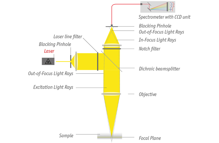
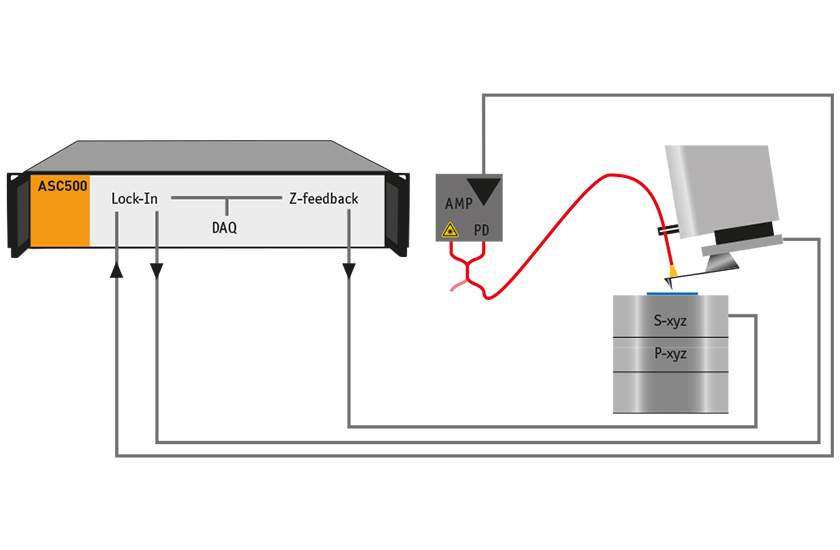
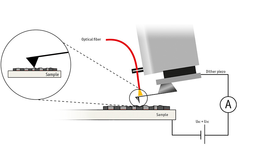
Confocal Microscopy (CFM) | Free-Beam Setup

Confocal microscopy is the most common instrumental technique in quantum optics to investigate semiconductor quantum dots, single molecules, color centers in diamond, photonic crystals, nanowires, quantum wells, 2D layered materials (graphene, chalcogenides) and many more. Often, the quantum nature of light emission requires cryogenic temperatures for the samples under investigation.

show more icon
fundamentals, confocal raman

Confocal Raman Microscopy

Historically, the Indian scientist C. V. Raman discovered in 1928 the - what was later called Raman - effect by demonstrating inelastic scattering of monochromatic light by highly viscous fluids. Only two years later, Raman was awarded the Nobel prize for his achievement. The Raman effect occurs if light impinges on a molecule and interacts with its electronic bonds. The spontaneous Raman effect is described as a three-level event, in which an incident photon first excites the molecule from ground state to a virtual state.

show more icon
fundamentals, cfm fiber based setup, sitemap

Confocal Microscopy (CFM) | Fiber-Based Setup

While the free-beam based attoCFM I offers a maximum amount of flexibility, its fiber-based counterparts attoCFM II and attoCFM III offer ultimate long-term stability onto the sample, and back up to the detector.

show more icon
fundamentals, cfm transmission

Confocal Microscopy (CFM) | Transmission

Transmission experiments in confocal microscopy sometimes also require filtering and shaping of the optical beam, and hence free-beam access instead of purely fiber-based can have quite some advantages in terms of flexibility.

show more icon
fundamental-scanning-gate-microscopes-grafik.jpg

Scanning Gate Microscopy (SGM)

SGM utilizes the ability of an AFM tip to influence the electrostatic properties of a sample locally. By applying voltage to the scanning tip, the tip acts as a movable electrical gate that can modify electrostatic potential for electrons in the sample and thus enables exploring electronic and transport properties at the nanoscale

show more icon

attocube-nano-positioning-logo-2022.svg

attocube systems AG
Eglfinger Weg 2
85540 Haar
Germany
 

Phone: +49 89 420 797 0
Fax: +49 89 420 797 201 90

Website: attocube.com
E-mail: info@attocube.com


Profile

attocube systems is the partner of choice for cutting-edge nanotechnology solutions for research and industry applications all over the world. The portfolio includes nano drives, an ultra precise displacement sensor, as well as microscope and cryostat systems which work close to the limit of what is technically and physically feasible.

attocube.com

Imprint Privacy Statement Careers

© 2021 attocube systems AG. All rights reserved.

X Products on notepadshow

Selected products

clear list
No products selected
Thank you for your interest in our products and your request.
Our Sales-Team will be in touch with you shortly.
Request info on selected products

cancel