Electron Diffraction
true nanometer accuracy for sample rotation
Electron diffraction is used to perform nano-crystallography of various materials and is of high relevance especially in the fields of chemical, pharmaceutical, and advanced materials research. The advantage of electron diffraction compared to X-ray crystallography is that electrons are less penetrating and therefore scatter more intensely. This allows the analysis of very thin layer samples which offer better availability than large crystals, and provide strong diffraction patterns in a short time. Electron diffraction analysis is usually performed as one of multiple techniques in electron microscopes, but due to the rising relevance, dedicated diffractometer concepts have emerged.
To achieve the highest resolution, the sample has to be positioned with the highest accuracy in vacuum conditions. Motion errors during the rotation of the sample, most importantly the radial runout, have to be minimized.
attocube's solution
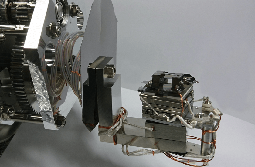
attocube offers a broad range of positioners to allow multi-axis sample positioning in extreme environments. Furthermore, attocube offers a unique error compensation feature, based on a technology invented by Synchrotron SOLEIL, which permanently reduces rotational runouts via a one-time calibration of the rotation stage. This rotation compensation feature offers accuracy down to 100 nm, while keeping a small footprint for flexible system integration.

