
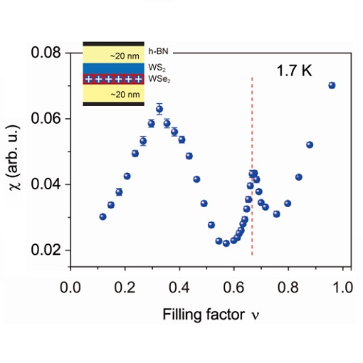
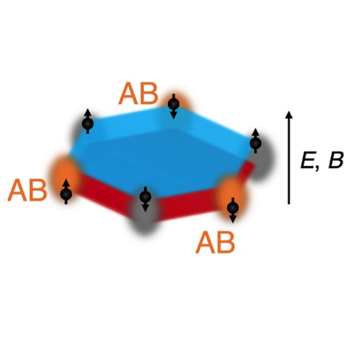
Competing magnetic interactions in moiré materials
The moiré materials provide a unique platform to study the effects of competing magnetic interactions, as electrons in semiconductor moiré materials are less strongly attracted to the moiré lattice sites compared to conventional solids. Here, the group of Kin Fai Mak and Jie Shan (Cornell University, USA) reports the evidence of strongly frustrated magnetic interactions in a Wigner-Mott insulator at 2/3 filling of the moiré lattice in angle-aligned WSe2/WS2 bilayers. Magneto-optical measurements with attoDRY2100 show that the net exchange interaction is antiferromagnetic for filling factors below 1 with a strong suppression at 2/3 filling. The suppression is lifted upon screening of the long-range Coulomb interactions and melting of the Wigner-Mott insulators by a nearby metallic gate electrode. The results can be qualitatively captured by a honeycomb-lattice spin model with an antiferromagnetic nearest-neighbor coupling and a ferromagnetic second-neighbor coupling. This study establishes semiconductor moiré materials as a model system for the lattice-spin physics and frustrated magnetism.
This measurement was realized with the attoDRY2100.
Further reading:
Y. Tang et al., Nature Nanotechnol. 18, 233 (2023)
Elucidated behavior of a ferroelectric-semiconductor phototransistor
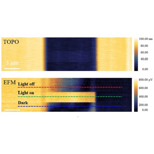
Low-light-level photodetectors (3LPDs) are key ingredients for quantum photonics devices, as well as in astronomy. To be compatible with complementary metal oxide semiconductors (CMOS) technology, they need to operate at low voltages, which is not the case as of now. The team lead by Zhihai Cheng (Renmin University of China, China) and Zhenxing Wang (National Center for Nanoscience and Technology, China) has fabricated and characterized low-light-level ferroelectric-semiconductor phototransistor (FSP) with an intrinsically high gain, featuring photo-induced ferroelectric switching. To unravel the photoresponse mechanism, they carried out in-situ EFM and KPFM on the FSP devices, in which the ferroelectric-semiconductor channels were identified by PFM. These correlative measurements have been realized by an attoAFM I microscope in an attoDRY2100 cryostat, with a KPFM upgrade and a PFM upgrade. This FSP demonstrates potential for novel generation of 3LPDs, due to its low operating voltage, high performance and simple architecture.
This measurement was realized with the attoDRY2100, and the attoAFM I.
Further reading:
J. Yang et al., Adv. Funct. Mater. 2022, 2205468 (2022)
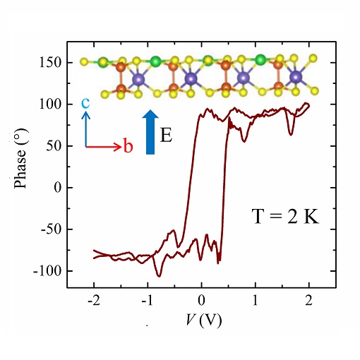
A van der Waals multiferroic
Coexistence of ferromagnetic and ferroelectric ordering in multiferroics makes these materials promising candidates for a next generation of storage devices. Collaboration of several Chinese universities studied a van der Waals (vdW) multiferroic CuCrP2S6 and found therein in-plane electrical and magnetic anisotropies with the same easy axis. Utilizing an attoAFM I microscope with PFM upgrade in an attoDRY2100 cryostat, Zhihai Cheng (Renmin University of China, China) performed piezoresponse force microscopy (PFM) measurements which indicate that the out-of-plane electric dipole originates from the antiferroelectric domain walls. Their findings - which include also the abilty to manipulate the magnons in CuCrP2S6 by electric field, magnetic field and temperature - demonstrate the potential of vdW multiferroics for applications in low-power and high-density non-volatile memories.
This measurement was realized with the attoDRY2100, and the attoAFM I.
Further reading:
X. Wang et al., Nature Commun. 14, 840 (2023)
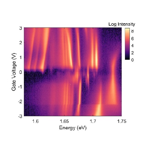
Let's Twist Again into Mott-Hubbard Physics
Layered two-dimensional (2D) materials are powerful playground for both quantum physics and nanotechnology. Lattice mismatch between two layers can create a moiré superlattice, which also affects electronic subsystem and often results in emergent electronic properties. This can also be realized with a homobilayer by a controlled twist of a precise angle.
The group of Kin Fai Mak and Jie Shan (Cornell University, USA) has become world leader in mastering the properties of 2D materials. Recently, they created a well-defined structure where two layers of WSe2 are twisted by an angle of 58°. Both layers are gated, so independent gate voltages can be applied to each layer, thus enabling additional control over the electron location between the two layers. In this way, they have turned the twisted WSe2 bilayer into a Hubbard-model system in the weak interlayer hopping limit. Furthermore, this Hubbard system can be tuned by electric and magnetic field thus rendering 2D moiré materials with flat electronic bands as easily tunable systems for studying strong electronic correlations.
To achieve these results, the team has utilized at best the main features of their attoDRY2100 cryostat, by monitoring the magnetooptical response at variable temperatures all the way down to 1.7 K.
This measurement was realized with the attoDRY2100.
Further reading:
Y. Xu et al., Nat. Nanotechnol. (2022)
Excitons in TMD for valleytronics
Semiconducting single-layer transition metal dichalcogenides (TMDs) have proven to be well suited for studying interplay between charge, spin and lattice, which is of interest for both fundamental physics and development of future applications. The broken inversion symmetry in TMDs and strong spin-orbit coupling lead to the spin-valley coupling of band edge electrons. In turn, a collaboration led by Xiaodong Xu (University of Washington, USA) has observed a new series of low-energy excitons, strongly coupled to phonons, in the photoluminescence (PL) spectrum of ultraclean single-layer WSe2, using an attoCFM I microscope in an attoDRY2100 cryostat. Their findings open a gate towards exploring collective phenomena in quantum optics using intrinsic donor-bound excitons in 2D materials and towards designing optical spin quantum memory.
This measurement was realized with the attoCFM I, and the attoDRY2100.
Further reading:
P. Rivera et al., Nature Commun. 12, 871 (2021)
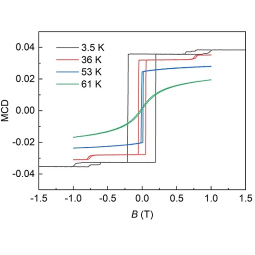
Harnessing the emergent potential of CrI3 flakes
For materials scientists it is not only essential to understand the properties of materials, but also to be subsequently able to design materials with desired properties that will in turn be implemented in devices. Van der Waals materials (vdWMs) have proven to be particularly rewarding when it comes to designing desired properties. Yet, among vdWMs there is a scarcity of magnetic materials, which would potentially be technologically useful for e.g. data storage or sensorics. CrI3 is one of the rare vdWMs that exhibits intrinsic magnetism. Even though this occurs only at low temperatures and the material is air-sensitive, CrI3 has become a notable playground for investigating and developing useful properties in vdWMs in recent years.
The group of Jie Shan and Kin Fai Mak (Cornell University, USA) have extensively studied magnetic ordering in CrI3 flakes, in a very application-oriented fashion. They have shown that interlayer antiferromagnetic coupling in CrI3 can be tuned up by almost 100% with pressure, before the transition to ferromagnetism occurs [1].
Moreover, in bilayer CrI3 they have demonstrated tunability of antiferromagnetic resonances in the range of tens of GHz by means of electrostatic gating, which indicates potential for ultrafast data storage and processing [2].
Furthermore, the basis has been laid for potential applications in magnetic actuation and sensing. The group has demonstrated magnetostriction in bilayer antiferromagnetic CrI3: in mechanical resonators made from CrI3 flakes, the resonant frequency depends on the magnetic state of the material [3].
Utilizing the property of controlling the interlayer magnetic order in CrI3 by electric field, the group has designed and tested a spin transistor based on CrI3 flakes. As magnetization configurations in this device are not controlled by spin current, but rather by gate voltage, the spin transistor can achieve a conductance ratio of ~400%, which is suitable for non-volatile memory applications [4].
Their results have been obtained with help of attoDRY1000 & attoDRY2100 cryostats, which have been used in conjunction with various experimental techniques like Raman spectroscopy, magnetic circular dichroism, magneto-optical Kerr effect, and tunnel magnetoresistance measurements.
This measurement was realized with the attoDRY1000, and the attoDRY2100.
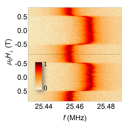
Signatures of a degenerate many-body state of excitons in van der Waals heterostacks
Condensed phases of excitons have previously been revealed by transport measurements in solid state systems with weak exciton binding, and consequently condensation temperatures below 1 K. Van der Waals heterostacks of semiconducting 2D materials are expected to host many-body phenomena at higher temperatures because of their peculiar screening properties and large exciton binding energies. The first optical exploration of such many-body phase diagrams of excitons has now been published by a collaboration of groups from Munich (Holleitner; Germany) and Münster (Wurstbauer; Germany). They used an attoDRY2100 closed cycle cryostat equipped with ANP nanopositioners to observe several criticalities in photogenerated exciton ensembles. The findings point towards a coherent many body quantum state, which survives to temperatures above 10K.
This measurement was realized with the attoDRY2100.
Further reading:
Phys. Rev. Research 2, 042044 (2020)
Isolating Hydrogen Gas inside H-BN Bubbles
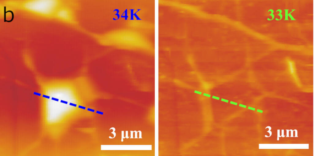
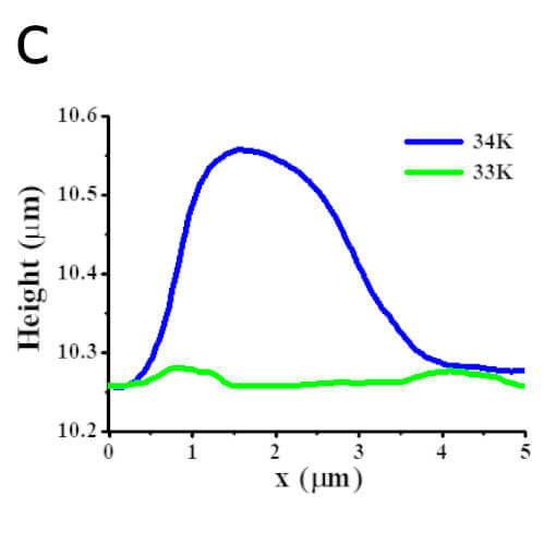
Storing small amounts of gas even on the atomic scale is extremely interesting for a lot of research fields. The choice of the barrier material plays an important role: It has to form bubbles to surround the stored gas, it has to be stable under extreme conditions, and it shall not interfere with the enclosed gas on chemical or physical terms. The group of Haomin Wang at the Chinese Academy of Sciences (Shanghai, CN) now presents new results on the production of isolated hydrogen inside hexagonal boron nitride (h-BN) bubbles via plasma treatment.
Low temperature atomic force measurements were carried out to prove that the surrounded gas is indeed hydrogen. Therefore, the authors used a cryogenic atomic force microscope, the attoAFM I, cooled by the closed cycle cryostat attoDRY1100, the 4 K version of the attoDRY2100. Setting exactly the measurement temperature and performing temperature sweeps gave the researches the possibility to show the bubble’s disappearance at a temperature of 33.2 K ± 3.9 K indicating a transition or disappearing of the enclosed gas. As this temperature is close to condensing temperature of H2 (33.18 K), the results point to the presence of atomic hydrogen inside the h-BN bubbles. The successful production of hydrogen inside the bubbles and presented results are a next step for hydrogen storage.
This measurement was realized with the attoDRY2100, and the attoAFM I.
Further reading:
Li He, et al; Nature Communications 10, 2815 (2019)
Enhanced coupling of NV-centre's spins and photons
Reliable quantum information systems require different quantum systems combining the best features of each of them. The most flexible and universal possibilities are offered by photons as mediator between localized qubits. Therefore, an effective coupling of solid-state based qubits to an optical photon is a fundamental requirement.
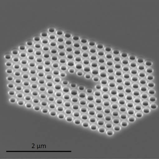
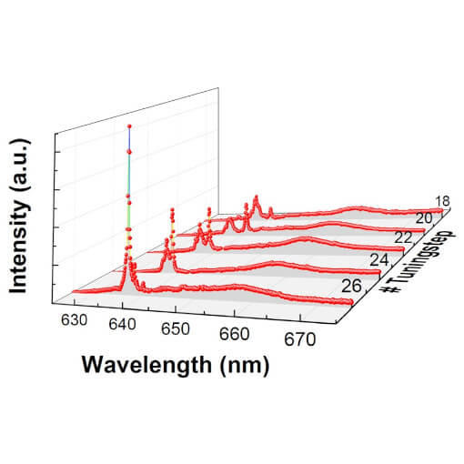
Nitrogen-vacancy centres feature a long spin coherence time and their spin can be optically initialized, manipulated and detected. However, only about three percent of their photon emission are channeled into the zero phonon line. This limits the rate of indistinguishable single photons and the signal-to-noise ratio of coherent spin-photon interfaces. The group of Christoph Becher at Saarland University (Saarbrücken, Germany) designed and fabricated a tunable two-dimensional photonic crystal cavity (figure 1) and reported an enhanced emission rate of one magnitude (figure 2). The tuning of the cavity mode into resonance with the zero phonon line of the NV centre was achieved by laser-induced adsorption of residual gas provided inside the vacuum tube of the closed cycle cryostat attoDRY2100. In-situ optical detection measurements allowed to control the actual tuning process. The result of their fabrication optimization and tuning is an almost tripled signal-to-noise ratio of the optical spin read-out. According to the authors even higher signal-to-noise ratio is possible using the presented fabrication technique and experimental setup.
This measurement was realized with the attoDRY2100, and the attoCFM IV.
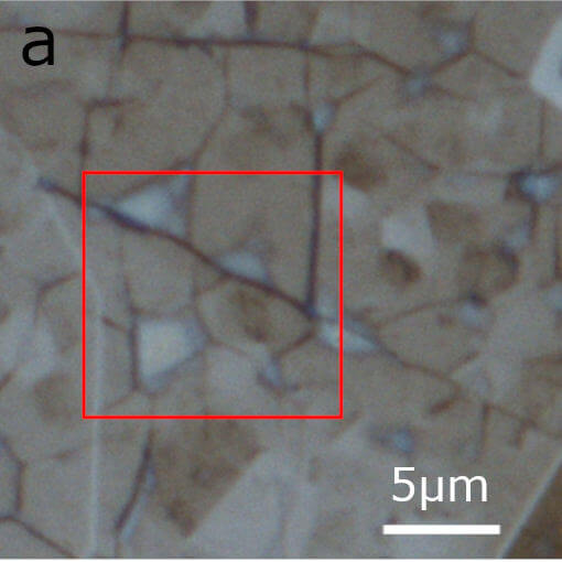
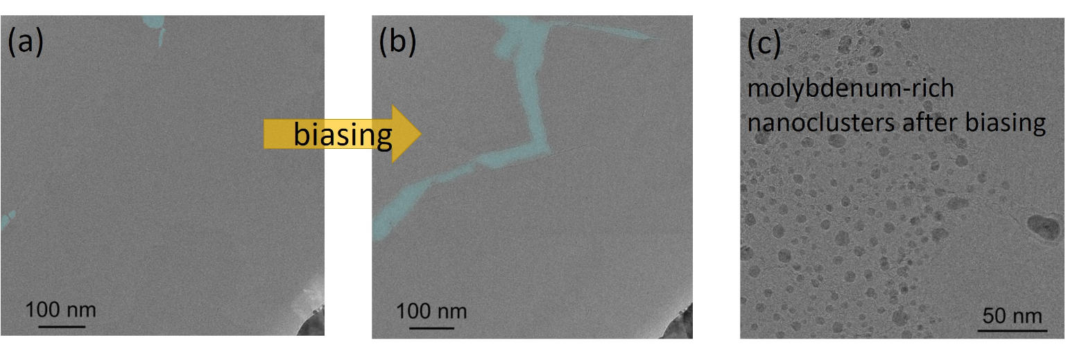
In-situ electrical biasing technique in MoS2
Due to their strong spin-orbit coupling and resulting large spin-orbit splitting in the valence band, layered transition metal dichalcogenides (TMD) are promising materials among the family of 2D materials for spintronic applications. The groups of Nathaniel Stern and Vinayak Dravid at Northwestern University (Evanston, Illinois, USA) used a film of monolayer MoS2 to present a new in-situ electrical biasing technique with transmission electron microscopy. They found that with an applied electric field a net vacancy flux towards the grain boundaries occurs. This vacancy flow results in a regions of Mo-rich nanoparticles aggregating near the voids (see figure c) which appear at strained regions around the grain boundaries (blue colored in figure (b)). The vacancy flow process saturates after several initial biasing cycles when the material reaches a stable state. To characterize these samples, they used the closed cycle cryostat attoDRY2100 combined with the attoCFM I and optical head to study structural dynamics by Raman spectroscopy.
This measurement was realized with the attoCFM I, and the attoDRY2100.
Further reading:
A.A. Murthy et al., ACS Nano 14, 2, 1569-1576 (2020)
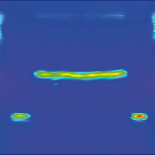
Collective electronic excitations of dipolar excitons
Photogenerated excitonic ensembles confined in coupled GaAs quantum wells are probed by a complementary approach of emission spectroscopy and resonant inelastic light scattering. The line scan of the photoluminescence energy in the image was measured at 7 K and covers the whole length of the circular trap with a diameter of 20 µm (x-axis). The inner electrode is circumvented by a ring shaped electrode at a different voltage. The gap of approx. 130 nm between the samples was created by e-beam lithography. The measurement was performed with an attoCFM III microscope inside a closed cycle attoDRY2100 cryostat.
This measurement was realized with the attoCFM III, and the attoDRY2100.
Further reading:
[1] S. Dietl, S. Wang, D. Schuh, W. Wegscheider, J. P. Kotthaus, A. Pinczuk, A. Holleitner, and U. Wurstbauer, Phys. Rev. B 95, 085312 (2017)
[2] J. Repp, G. Schinner, E. Schubert, A. K. Rai, D. Reuter, A. D. Wieck, U. Wurstbauer, J. P. Kotthaus, and A. Holleitner, Applied Physics Letters 105, 241101 (2014)
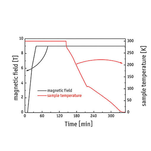
The perfect dry VTI: excellent temperature stability and field cooling
Investigating samples at variable temperatures and magnetic fields is a common task in physics and materials science. Using the attoDRY2100, a closed-cycle cryostat with superconducting magnet, researchers can easily access the whole phase space of temperature between 1.65 K and 300 K as well as magnetic field, usually -9 Tesla to +9 Tesla (others on request) without compromises on performance. The cooldown time of an insert is about 3 .. 7 hours.
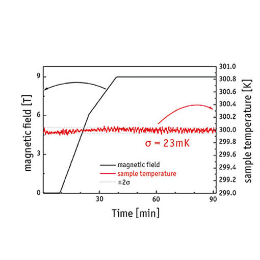
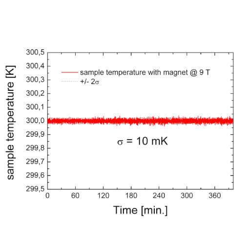
The attoDRY2100 is not only capable of reaching the full magnetic field even at 300 K sample temperature with an excellent temperature stability (10 mK), but also features the possibility of field cooling a sample. The whole temperature and magnetic field control is automated, accessible via the integrated touchscreen or remotely via LabVIEW or a dll.
In the measurements shown in the first figure, the attoDRY2100 with an atto3DR transport measurement insert was first set to a target sample temperature of 300 K, and then the magnetic field was ramped up from zero Tesla all the way to the full 9 Tesla. This took about 40 minutes. During this process, the sample temperature was stable to within sigma = 23 mK (Fig. 2). At 9 T and 300 K, the temperature stability was even better at sigma = 10 mK over more than 6 hours, see figure three. Subsequently, the sample was field cooled at 9 T back down to base temperature, which took about 3.5 hours.
This measurement was realized with the attoDRY2100.