

THz Plasmon Polaritons
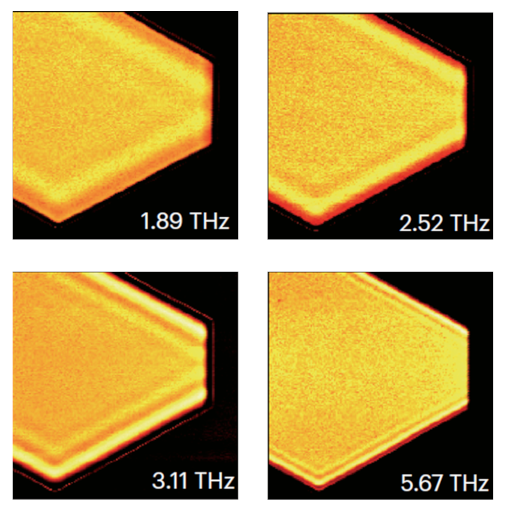
Plasmon polaritons are quasiparticles resulting from the coupling of surface plasmons with light. Such Polaritons possess tremendous potential for investigating essential material properties and advancing the field of nanophotonics by enabling the creation of innovative devices. However, the direct observation of ultraconfined in-plane anisotropic plasmon polaritons has proven to be a scientific and technological challenge until now. With this publication, the authors used s-SNOM to image ultraconfined in-plane anisotropic THz plasmon polaritons in a narrow-bandgap semiconductor with strong anisotropy. By placing the platelets above a gold layer, the hybridization of plasmon polaritons with their mirror image enhances the direction-dependent propagation length and confinement of the polaritons. The THz s-SNOM images of the Ag2Te/SiO2/Au heterostructure reveal up to three narrow polariton fringes parallel to the edges. These findings expand the control and manipulation of polaritons, offering potential for nanoscale photonic devices and applications.
The study demonstrates the use of THz plasmon polaritons for measuring anisotropic charge carrier masses and damping.
This measurement was realized with the THz-neaSCOPE+s.
Further reading:
Chen et al., Nature Materials 84, 2869 (2023)
Laser THz Emission Microscopy
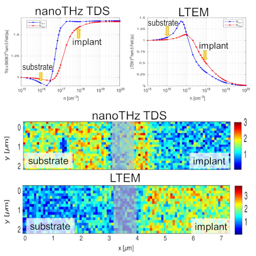
s-SNOM has revolutionized subwavelength optics by coupling electromagnetic radiation to a sharp subwavelength metal tip, held near a surface, and measuring the scattered radiation. This technique has had a significant impact in the infrared and terahertz regions of the spectrum. However, coupling short-wavelength radiation to the nanoscale tip has been challenging, hindering the study of wide-bandgap materials such as Si and GaN. In this study, the first s-SNOM measurement exceeding 3?eV photon energy was achieved, allowing the use of tightly focused blue light for nanoscale resolution. This technique, known as laser terahertz emission microscopy (LTEM), offers exciting new possibilities for the application of s-SNOM methods to wide-bandgap materials.In summary LTEM spectroscopy and imaging, providing an avenue to directly observe charge carrier properties in materials not amenable to THz s-SNOM techniques.
This measurement was realized with the THz-neaSCOPE+s.
Further reading:
Pizzuto et al., Light: Science and Applications 12, 96 (2023)
THz Polaritons Nanoimaging
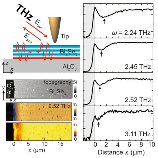
Plasmon polaritons in metals, doped semiconductors and 2D materials have wide application potential for field-enhanced spectroscopies, sensing, imaging, and photodetection. Although polaritons have been observed by many IR s-SNOM studies, real-space imaging of propagating THz polaritons has been missing so far. This study brings the analytical power of s-SNOM to the THz spectral region. In this study, spectroscopic THz near-field images reveal polaritons with up to 12 times increased momenta as compared to photons of the same energy. From the images the authors determine and analyze the polariton dispersion, showing that the polaritons can be explained by the coupling of THz radiation to various combinations of Dirac and massive surface carriers, massive bulk carriers and optical phonons.
THz s-SNOM provides critical insights into the nature of THz polaritons in topological insulators and establishes instrumentation and methodology for imaging of THz polaritons.
This measurement was realized with the THz-neaSCOPE+s.
Further reading:
Chen et al., Nature Communications 13, 1374 (2022)
Electron Motion in Nanostructures
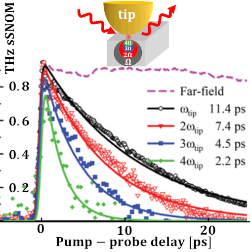
Charge transport in nanomaterials is the key process in many applications in nanoelectronics. An efficient tool for the characterization of charge transport in semiconductors nanostructures is terahertz (THz) spectroscopy, which involves contactless probing of the conductivity. Another more local investigation tool is THz s-SNOM which combines the THz frequencies with nanoscale resolution on an AFM. This study combines ultrafast pump-probe nanoscopy with THz s-SNOM which allow in-depth understanding of the nanoscale electron motion inside the nanobars. In addition, this study reveals that electrons are submitted to additional forces (band bending) close to the nanobar surfaces, which greatly enhance confinement of electrons at the picosecond timescale.
THz s-SNOM in combination with ultrafast pump-probe nanoscopy provides unique tool for the investigation of electron motion in nanostructure surfaces.
This measurement was realized with the THz-neaSCOPE+s.
Further reading:
Pushkarev et al., Advanced Functional Materials 5, (2022)
Nanoscale Terahertz Microscopy
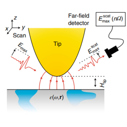
Terahertz (THz) radiation has become an important diagnostic tool in the development of new technologies. However, the diffraction limit prevents terahertz radiation (λ ≈ 0.01–3 mm) from being focused to the nanometer length scale of modern devices. In response to this challenge, terahertz scanning probe microscopy techniques based on coupling terahertz radiation to subwavelength probes such as sharp tips have been developed. These probes enhance and confine the light, improving the spatial resolution of terahertz experiments by several orders of magnitude. In this Review, THz s-SNOM is compared with other probe microscopy techniques that achieve spatial resolution on the scale of micrometres to ångströms, with particular emphasis on their overarching approaches and underlying probing mechanisms.
THz s-SNOM provides unique and complementary information to conventional IR s-SNOM nanoscopy.
This measurement was realized with the THz-neaSCOPE+s.
Further reading:
Cocker et al., Nature Photonics 15, 558–569 (2021)
Coplanar Microwave Resonators
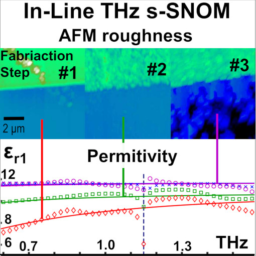
Superconducting quantum circuits are one of the leading quantum computing platforms. To advance superconducting quantum computing to a point of practical importance, it is critical to identify and address material imperfections that lead to decoherence. In this study THz s-SNOM probes the local dielectric properties and carrier concentrations of wetetched aluminum resonators on silicon, one of the most characteristic components of the superconducting quantum processors. We ?nd that the permittivity and carrier concentration of silicon in wetetched regions are modi?ed, leading to increased THz s-SNOM scattering compared to high-resistivity silicon. In conclusion, THz s-SNOM combines microscopy with local THz spectroscopy and can be used to identify processing-induced inhomogeneities that limit device function.
In-line THz nanoscopy is a non-invasive method to quantify and identify potential loss channels in quantum devices without the need of electrical contacts.
This measurement was realized with the THz-neaSCOPE+s.
Further reading:
Guo et al., Appl. Phys. Lett. 119, 091101 (2021)